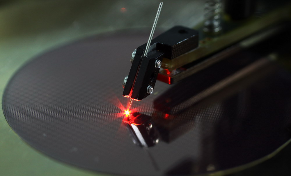
Guide: An LED chip, also known as a light-emitting diode (LED) chip, is the core component of an LED light. It is often referred to as a PN junction, and its primary function is to convert electrical energy into light energy. But what are the typical sizes of LED chips, and how are they manufactured? Let's take a closer look at these details.
What Sizes Do LED Chips Come In:
High-power LED chips typically come in three common sizes: 38x38 mil, 40x40 mil, and 45x45 mil. These measurements are standard for 1W high-power LED chips. A "mil" is a unit of length equal to one-thousandth of an inch. For reference, 40 mils are approximately 1 mm. The size of the chip directly affects its ability to handle current and power. In general, larger chips can support higher currents and greater power. However, the material and manufacturing process also play a significant role in determining the performance of the LED. For instance, two LEDs of the same size might have different power ratings—some may handle up to 3W, while others only reach 2W.
The Manufacturing Process of LED Chips:
The production of LED chips is generally divided into two main stages. First, a gallium nitride (GaN)-based epitaxial wafer is created on a suitable substrate. This is typically done using a metal organic chemical vapor deposition (MOCVD) system. The process involves preparing the necessary materials and high-purity gases, then depositing layers of semiconductor material according to precise specifications. Common substrates include sapphire, silicon carbide, silicon, and even GaAs, AlN, and ZnO in some cases.

The MOCVD process uses gaseous precursors, such as group III organometallic compounds and ammonia (NH3), which react on the surface of the substrate to form the desired semiconductor layers. By controlling factors like temperature, pressure, and gas concentration, the composition and quality of the deposited material can be precisely managed. This step is crucial in creating high-quality LED wafers.
Once the epitaxial wafer is ready, the next stage involves processing the electrodes of the LED’s PN junction. This includes several key steps such as cleaning, evaporation, yellowing, chemical etching, fusion, and grinding. After that, the wafer is diced into individual chips, tested, sorted, and finally packaged to produce the finished LED chips.
If the cleaning process is not thorough, or if the evaporation system is not functioning properly, issues such as electrode peeling, discoloration, or abnormal gold bubbles can occur. During the evaporation process, the LED chip is sometimes held in place with a spring clip, which can leave a small indentation that must be removed during visual inspection.
The yellowing process includes steps like baking, applying photoresist, exposing it to light, and developing. If the development is incomplete and the mask has holes, excess metal may appear in the light-emitting area, affecting performance. Additionally, in the early stages of chip production, various processes such as cleaning, evaporation, and etching require handling with tools like tweezers, flower baskets, and carriers, which can sometimes lead to minor scratches on the chip’s surface.
HP Chromebook X360 11 G3 EE,HP Chromebook X360 11 G3,HP Chromebook X360 11 G3 keyboard,HP Chromebook X360 11 G3 Palmrest
S-yuan Electronic Technology Limited , https://www.syuanelectronic.com