Abstract This device utilizes the caller ID service to decode the caller ID data through the FSK decoder chip MC14LC5447. It uses AT89C2051 MCU for data acquisition and data storage. The DLL dynamic link library controls USB203 (8-bit parallel input USB transmission module) to complete the pair. Store the data and analyze it. Through the device, the collection, analysis and processing of incoming call data can be completed, the improved software interface is used for data transmission, and interface functions for VC, VB and DELPHI language programming environments are provided.
This article refers to the address: http://
Keyword calling number display Frequency shift keying (FSK) MCU USB interface design USB203
Caller ID is a new service launched by the telecommunications department in recent years - displaying the phone number and call time of the called party. Caller ID telephones and caller ID products are widely used and their technology is quite mature.
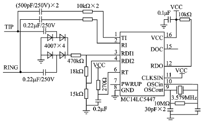
Figure 1 Caller ID signal decoding module circuit principle
Traditional caller ID messages only display data on their own phones, and they cannot provide data to a computer or other device. Therefore, it is very necessary and practical to develop the interface between the caller ID telephone and the computer and the related data acquisition system.
The device is divided into four sub-module designs, which are caller ID signal decoding module, signal acquisition module, telephone signal processing module and USB transmission module. The USB transmission module is called by the interface function, and the caller ID number can be obtained through the interface function.
1 Caller ID signal decoding module design
The caller ID signal decoding module is mainly implemented by the FSK decoder chip MC14LC5447, and its principle is shown in Figure 1. The caller ID output has two signals, DOC and DOR. The difference in the data format is that the DOC processes the channel occupancy signal of the caller ID (composed of 300 consecutive 0, 1 alternating bits of the leading), and the DOR is the decoded data of the chip, and there is no deletion. Since the difference between the two signals is only the difference of the channel occupancy signals, then the use of DOC will be more convenient than DOR, because the data stream of the DOC is the data stream of the caller ID.
There are two ways to detect data, RDO and CDO. RDO is the ringing detection output. When there is no ringing, RDO outputs a high level. When there is ringing, RDO outputs a low level until the ringing ends; CDO is the carrier detection output. When there is no carrier, CDO output High level, when there is a carrier, CDO outputs low until the end of the carrier. RDO is not limited by the chip switch (PWRUP) signal, and when the chip switch is high, it will remain high regardless of whether the carrier signal is detected or not.
TIP and RING are telephone lines, and the connection is not required, and can be connected at will. The difference between the TIP line and the RING line is that the voltage of the load is different, the voltage of the TIP line is a negative voltage, and the voltage of the RING line is a positive voltage. The pressure difference between the two lines is 60 V or 48 V (regional difference).
The PWRUP signal ground can be used as the test end (PWRUP is grounded to keep the chip always on). The DOR signal always has an interference signal in this test, but when there is an incoming call, the signal is normal. In order to improve the stability of the system, DOR is generally not used as a data signal output. The CDO requires PWRUP support. If the PWRUP is grounded and the chip is always in operation, the CDO can be used as a trigger signal. Considering the low power requirements of the system, the chip must be turned off when not in use; however, the CDO has no signal when the chip is off, and the RDO is not controlled by the power supply and is easier to use. In addition, turning off the chip can also enhance the stability of the system while improving the security and reliability of the data.
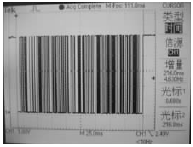
Figure 2 Caller ID timing
Figure 2 shows the test results of the DOC signal (acquisition results in a digital oscilloscope). Due to the time-division segmentation, only the data reference is made, and the time frame and the check frame are not the result of one acquisition. Figure 3 is the timing after the graphical processing.
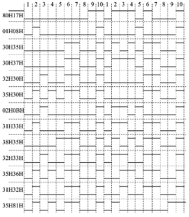
Figure 3 Caller ID timing (after computer graphics processing)
It can be seen from the sampling timing diagram that the caller ID waveforms are arranged in an asynchronous serial data format, with 0 as the start bit and 1 as the stop bit; but unlike the various materials, there is no field check bit, and the arrangement should be each The 9th bit of the packet, except the type field and length field and the last check field. It can be seen that the collected data has no check digits. Caller ID packets are available at 1 200 bps and are also available from digital oscilloscopes, with a data footprint of 830 μs per bit (since the time accuracy of a digital oscilloscope cannot be accurately adjusted to 1 μs, it can only be accurate to 830 μs) Basically the same rate as 1 200 bps (1 s ÷ 1 200 bits ≈ 833.333 μs), so the caller data is stable. It should be noted that after the end of the incoming call data packet, that is, after the end of the sampling packet 81H, there is actually a data signal, and each bit takes up 410 μs and the data rate is 2 400 bps. This signal is an idle signal, so it needs to be filtered by the filter during acquisition.
2 signal acquisition module design
As a study of the output data, the signal demodulated by the MC14LC5447 is an asynchronous serial signal, and the data rate is 1 200 bps. The serial port mode 1 of the microcontroller can be used for data reception. The algorithm is described in reference [1]. In addition to data acquisition, the MCU unpacks the serial data packet and restores the data.
Most of the main interrupt routines are waiting for the interrupt response of the serial program. The first thing you need to receive is the length field of the caller ID packet. The advantage of receiving the length field is that you can dynamically receive incoming call packets without having to wait for receiving each time. Fixed length. Although the length of the caller ID packet cannot be greater than a certain fixed length, according to the length field of the incoming call data packet, the data is dynamically received, so that the collected data is easier to process, and the interference signal at the end of the data packet can be filtered again, thereby reducing The load of other programs.
Of course, the data can be separated and processed by the single-chip microcomputer, but for the analyzability of the package, the MCU does not do other work except data acquisition.
The data obtained at a time is as follows:
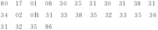
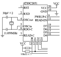
Figure 4 Principle of the data acquisition module
Figure 4 shows the principle of the data acquisition module. The DOC signal output of the MC14LC5447 is connected to the 2nd pin of the AT89C2051 (serial input port); the RDO signal output of the MC14LC5447 is connected to the 6th pin of the AT89C2051 (external to the AT89C2051). Interrupt 0); The 9th pin of the AT89C2051 is connected to the 7th pin (PWRUP) of the MC14LC5447 to control the MC14LC5447 on and off. The 7th pin of the AT89C2051 is connected to the USB device status output port, the 1st pin is also connected to the status output port of the USB device, the 11th pin is connected to the status input port of the USB device, and the data line is connected to the parallel data input of the USB device. mouth. The 12th and 13th pins require an external pull-up resistor.
The solution implemented by the single-chip microcomputer has many advantages over the scheme of the digital logic circuit. Mainly there are small chances of error, storage control function, convenient, flexible replacement.
The use of store-and-forward schemes improves the security of data transmission. Since the USB203 has no USB interrupt function, receiving data can only be implemented in a program loop, but improper use of loops increases the burden on the system.
3 telephone signal processing module design
The hook signal can be obtained by the telephone hook line.
After detection, there are two signals on the hook: one is a 22~27 V sine wave signal, which is located on the 5th and 6th pins of the hook spring; the other is a 15~20 V negative sine wave signal, which is located at the fork spring 3rd. , 4 pins. The first and second pins are signal outputs. When the shrapnel on the hook spring is not depressed, the first and second pins are connected to the fifth and sixth pins, and the signal is a positive alternating current signal, which means that the off-hook is off; when the machine is on-hook, the spring on the hook spring is pressed. At this time, the first and second pins are connected to the third and fourth pins, and the signals on the first and second pins are negative AC signals. This signal is converted to logic 0, 1 level, that is, the signal is logic 1 when off-hook, and logic 0 when on-hook, the circuit principle is shown in Figure 5.
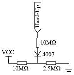
Figure 5 fork spring signal processing principle
Filtering is performed by a voltage dividing circuit and a diode, and the negative half cycle signal is filtered by the diode. Due to the 10 MΩ resistor divider, the output level is around 1 V. After testing, the USB status input pin requires 1.6 V or more to consider the input signal to be logic 1, while below 1.6 V is considered to be logic 0.
The off-hook input signal is a sine wave. After passing through the rectification and filtering circuit, it can output a level signal of about 2.6 V to the USB device, and the signal is a stable logic 1.
The hang-up signal with a negative hang-up signal can output a 260 mV level signal to the USB device through the rectification filter circuit, and the signal is a stable logic 0.
4 USB transmission module design
The USB transmission module uses USB203 as the transmission interface, as shown in Figure 6. The advantage of using this module is that it is a parallel-to-serial conversion transmission module, and has 4-bit control signal input and 4-bit control signal output, and provides DLL library files, which is convenient for secondary development; but this device does not have The interrupt control method is used, so reading data will be the bottleneck of the system. However, a large amount of data acquisition is not used in the system, and the data length is only 26 bits. Even for composite caller ID packets of other lengths, the length is not more than 1 000 bits, so whether it is for high speed transmission is not important. The reason why this system uses USB is that USB is easy to use and supports hot plugging, which is more advantageous for devices using RS232 communication port; in addition, USB uses 5 V power supply to provide power for external devices, saving external devices. The power supply section reduces the size of the external device.
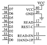
Figure 6 USB transmission module circuit principle
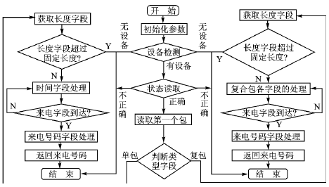
Figure 7 USB interface program algorithm flow chart
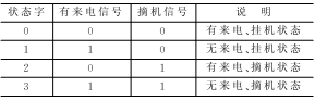
In the DLL, the USB_CID function needs to be established. Without parameters, the caller number in the processed incoming call packet is directly returned, and the corresponding error code is returned when there is no number. It should be noted here that although the microcontroller program is variable length storage, there are still errors due to the transmission of the caller ID data packet. When an incoming call occurs, the data packet will be between the first and second ringing. If the caller hangs up the call, the incoming call data packet will no longer be sent; or the called party picks up the phone and will also lose the incoming call data packet, then the incoming call will be lost. The packet will be stored a part, and the microcontroller will continue to wait for reception without restarting. When the next incoming call arrives, the new incoming call packet will continue to be stored until the first incoming call packet length is met before the end of the incoming call, and the entire data packet will be retrieved by the interface program and judged to be in error. If it is a composite package, the error will be excluded before the incoming call number data packet, but if there is an error in the incoming call data number data packet, the received number will be sent, and the display may be garbled. The algorithm flow is shown in the figure. 7 is shown. Table 1 gives the definition of the status word.
Table 1 Status word definition
5 Conclusion
The information interface USB interface design is the interface between the caller ID telephone and the computer and the related data acquisition system. It uses the interface technology and computer software technology to realize the display or storage of the caller ID and other related information on the computer, and can make calls according to the basic information. Classification statistics of numbers. These data will play an important role in improving the quality and efficiency of relevant departments, and can also provide reference information to relevant decision-making departments in a timely manner.
The device completes data acquisition and data transfer, and completes the separation of related data through a software interface. The caller ID technology was studied in detail, and the microcontroller program was programmed and written in VC++. The device can be embedded not only in the phone but also as a single module, so the system has a wide range of practical value.
Sleeping Eye Mask,Cold Eye Mask ,Cooling Face Mask ,Spa Eye Mask
Hair Weaving & Hair Weft Co., Ltd. , http://www.nboutdoors.com