0 Preface
Voice communication is one of the most commonly used communication methods in digital communication systems. An excellent voice encoding and decoding algorithm can more effectively save bandwidth resources and improve frequency utilization. Now speech coding technology can be widely used in many military fields such as voice multiplex transmission, satellite communication, and confidential communication. AMBE-2000 is a high-performance, low-power real-time codec chip based on advanced multi-band excitation (advanced mulTI-band excitaTIon) speech coding algorithm, and its compression ratio Adjustable from 2 000 to 9 600 b / s, with various functions such as forward error correction (FEC), voice activation detection (VAD), and dual tone multi-frequency (DTMF) signal detection.
1 System introduction
The main function of this voice system is to realize the conversion between digital voice and analog voice and process the coding and decoding of voice data, reduce the transmission rate of voice data, improve the frequency resource utilization rate of the system, and must meet the interface requirements of the information system. The analog voice part is connected to the headset microphone group, the digital part compressed data stream is connected to an external processor, and the decompressed data stream is used to transmit voice quantization information over a long distance. The block diagram of the entire voice system is shown in Figure 1.
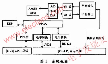
When the voice is sent, the voice processing board performs A / D sampling and quantization on the input analog voice, and compresses and packs the voice codec chip through the CPCI bus or LVDS serial bus to the information processor for subsequent processing; or through high-speed RS 422 The serial port compresses the voice quantized information transmitted from a long distance and sends it to the information processor through the CPCI bus or LVDS serial bus for subsequent processing. Welcome to reprint, this article comes from the electronic enthusiast network (http: //)
When receiving voice, the compressed data is received through the CPCI bus or LVDS serial bus. After decoding by the voice codec chip, the voice is converted into an analog signal through D / A conversion; or the received compressed data is decompressed and passed through high-speed RS 422 The serial port is transmitted over a long distance.
2 AMBE-2000 functions and features
AMBE-2000 chip is an improved product of AMBE-1000. Compared with AMBE-1000, its voice compression algorithm is more optimized, voice quality is higher, and the minimum coding rate is also reduced from the original 2 400 b / s to 2 000 b / s. In terms of hardware and interfaces, several improvements have been made, and the efficiency and reliability of its compression coding and forward error correction coding (FEC) have been improved. Small internal calculation and low power consumption. Its algorithm complexity is 13 MIPS (millions of instructions per second), which can achieve lower power consumption: only 65 mW at 3.3 V, and only O.11 mW at deep sleep.
In the simple model, AMBE-2000 is seen as two separate originals, encoder and decoder. The encoder receives the speech quantization information (16-bit linear, 8-bit A-law or 8-bit μ-law) and outputs the compressed data stream to the channel at the desired rate. Conversely, the decoder receives the channel compressed data stream and synthesizes speech quantization information. The time control of the AMBE-2000 encoder / decoder interface is completely asynchronous. Usually the A / D and D / A chips are connected to the voice interface. The input and output voice data streams must be the same. Format (16-bit linear, 8-bit A-law, or 8-bit μ-law). This system adopts AMBE-2000 and A / DD / A chip adopts AD73311 with 16-bit linear sampling to maintain compatibility with the originally designed AMBE-1000 based voice system. The old voice system based on AMBE-1000 uses a 16-bit linear A / D and D / A chip TI32044, which is too large and has high power consumption, and uses a series of peripheral chips with the same disadvantages, which is not suitable for low power consumption. , The development trend of small volume.
3 Interface design of AMBE-2000 and A / DD / A chip
The format of the voice data stream between the A / DD / A chip and AMBE-2000 should match, that is, to have a unified format (16-bit linear, 8-bit A law, or 8-bμ law), under normal circumstances , 16-bit linear components are recommended. In this design, the AD73311 from AD is used. The voice interface of AMBE-2000 can be set to communicate exclusively with AD73311 by configuring hardware pins 84, 85 (CODEC_SEL [1-0] = 01b) Therefore, the combination of AMBE-2000 and AD73311 will make the circuit design relatively simple.
AD73311 main features:
(1) Low-power 16-bit A / DD / A converter, input / output sampling rate and gain can be controlled by software, which can provide 70 dB signal-to-noise ratio in the voice band range. It is simple and efficient to transfer voice data and receive control commands through the serial port.
(2) The input analog audio signal passes through the variable gain amplifier, the A / D converter is converted into a digital signal, and is output through the serial port; otherwise, the digital stream from the serial port is converted into an analog signal, and then output through the variable gain amplifier.
(3) There are two main working modes of AD73311: programming mode and data mode. After the chip is reset, it is in the default programming mode. At this time, you can write the control word to the control register through the serial port to set the working state. It should be noted here that the configuration word of the AD73311 in the 3 V low power consumption state (as shown in Figure 2) should be set to the corresponding format.
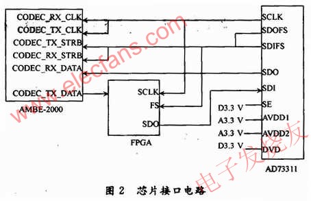
(4) After power-on reset, the CODEC_TX_DATA signal of AMBE-2000 should be isolated from the serial input of AD73311, and keep it for about 365 ms. At this time, use FPGA to configure AD73311, the configuration word is as follows:
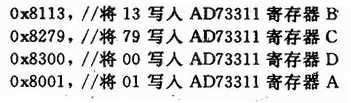
After setting, register A writes Q1, which means to enter the "data mode", the CODEC_TX_DATA signal of AMBE-2000 should be connected with the serial input of AD73311, and normal data transmission can be carried out.
4 AMBE-2000 and channel interface design
AMBE-2000 requires the encoder to be read by the controller every 20 ms. After the reset, the EPR changes from high to low when the initial frame is ready, and then 1 frame of data is prepared every 20 ms. Accordingly, the external controller also needs to read 1 data frame every 20 ms.
The EPR pulse appears once every 20 ms, which is also an important basis for judging whether the AMBE-2000 is working normally. The whole process of reading data is:
(1) Wait for less than 20 ms;
(2) Send frame synchronization signal, read AMBE-2000 serial output data of one frame;
(3) If the received data is not 0x13EC, it means that it is not the data frame header. Discard this frame and re-execute step (2).
(4) If the data of chestnut receiving thistle is 0x13EC, then read the remaining 23 words of this packet.
In this design, FPGA is used as an external controller. The FPGA generates input / output frame synchronization signals, input / output clock signals, and serial input data of AMBE-2000, and exchanges data with AMBE-2000 according to the timing relationship required by AMBE-2000.
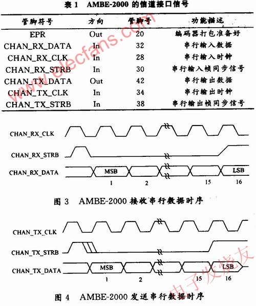
Table 1 lists the characteristics of AMBE-2000's channel interface signals, and the data transmission mode with the external controller is shown in Figure 3 and Figure 4.
5 System peripheral interface design
The peripheral interface of the system includes: CPCI interface circuit; conversion circuit between LVTTL and standard LVDS level signal; conversion circuit between LVTTL and standard RS 422 level signal; analog circuit.
5.1 CPCI interface circuit
The use of CPCI-specific bridge chips can avoid complex PCI protocols and quickly develop products. Therefore, the high-performance dedicated bridge chip PCI9054 of PLX is used to realize the CPCI interface design. Use the IP core in the FPGA to generate dual ports and establish the glue logic with the CPCI part to complete the CPCI interface design.
5.2 Conversion circuit between LVTTL and standard LVDS levels
In this system, in addition to the standard CPCI bus form to realize data exchange between the digital part compressed data stream and external communication equipment, a LVDS serial bus mode transmission is also required, which requires a transmission rate of up to 100 Mb / s. The system uses MAX9129 and MAX9122 bus low-voltage differential signal drivers as drivers for LVTTL and standard LVDS level signal conversion circuits.
5.3 Conversion circuit between LVTTL and standard RS 422 level
The data exchange between the decompressed voice data stream and external digital audio equipment is transmitted by the standard RS 422 serial bus, which requires a transmission rate of up to 5 Mb / s. This system uses the MAX3491 low-power RS ​​485 / RS 422 transceiver as the driver of the LVTTL and standard RS 422 level signal conversion circuit, which is used for data transmission at a long distance. Each chip of the MAX3491 contains a driver and a receiver, and the maximum transmission rate can reach 10 Mb / s.
5.4 Analog circuit
The analog amplifier circuit includes op amps and some container components. The main function is to use a high-performance low-noise amplifier to adjust the gain of the input / output voice signal through a potentiometer or an appropriate proportional resistance.
The audio interface circuit of this design adopts active balanced input / output voice transmission mode, which plays the role of differential mode amplification and common mode suppression and improves anti-interference ability. In the early days of audio production, people often use transformers to correct the ground potential difference between different devices and cancel the electrical noise generated in the cable line. It can also connect active equipment with unbalanced high impedance characteristics and balanced transmission lines with lower impedance characteristics. However, transformers increase the cost and increase the weight of the system. Transformers sometimes cause system distortion. Therefore, designers continue to seek ways to remove the transformer, and as a result, they have found active balanced input / output circuits.
6 Conclusion
The voice system structure adopts 6U CPCI standard board, half-duplex working mode, within the voice bandwidth of 300-3400Hz, the intelligibility of voice words is greater than or equal to 90%, the intelligibility of speech sentences reaches 100%, and the tone is natural. The pronunciation is clear and it is a high-quality voice system.
High Intensity Focused Ultrasound (HIFU) technology is to focus ultrasound on a single point to produce high energy, function on the dermis and SMAS layer of skin, stimulate the proliferation and recombination of collagen, effectively achieve the effect of compact contour and smoothing lines.
Focused ultrasound does not heat the skin surface, nor does it need to pass through the skin as a medium for the transmission of laser energy, so it does not affect the tissue on the skin surface and the tissue through which the laser passes, of course, there will be no excessive heat residue on the skin surface. In this way, the epidermis will not be affected by heat, which can reduce the Eastern people's thermal reaction easily, and greatly reduce the chance of scald. Focused ultrasoundtherapy produces thermal coagulation points in the SMAS layer, and the thermal effect diffuses outward from the coagulation points, so the heat source is concentrated in the SMAS layer to be treated. It can produce more collagen denaturation.
HIFU Piezoelectric Ceramic Parts
Ultrasonic Transducer Component,Piezo Crystal For Vibration Transducer,Piezoelectric Ultrasonic Rings,High Power Ultrasonic Machining
Zibo Yuhai Electronic Ceramic Co., Ltd. , https://www.yhpiezo.com