The UBA2028 is a compact fluorescent electronic ballast control and drive high voltage power IC from NXP Semiconductors. This advanced chip integrates the same CFL electronic ballast control circuit as the UBA2014, along with two half-bridge power MOSFETs, making it a complete solution for dimmable 5–25W CFL applications. It provides pre-heating, ignition, and dimming control, while also offering system protection features to ensure reliable performance.
Basic Structure and Pin Function
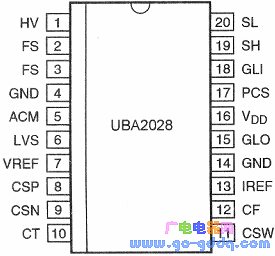
The UBA2028 is available in an S020 package, with a compact body width of just 7.5mm. The top view pin layout is shown below:
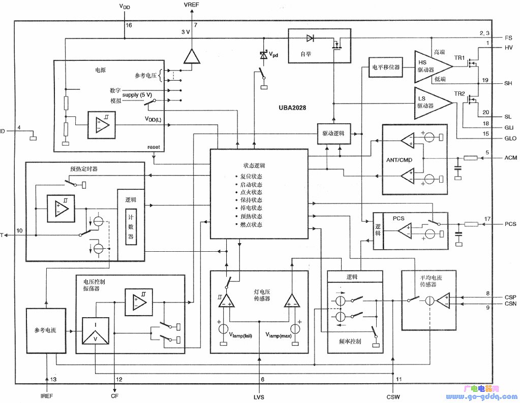
The internal architecture of the UBA2028 consists of the UBA2014 ballast controller and two N-channel power MOSFETs (TR1 and TR2), which together form a half-bridge configuration. The block diagram is illustrated below, along with a detailed pin function table.
| Pin | Symbol | Features |
| 1 | HV | High voltage input |
| 2 | FS | High-end switch floating power supply |
| 3 | FS | High-end switch floating power supply |
| 4 | GND | Ground |
| 5 | ACM | Capacitive mode input |
| 6 | LVS | Lamp voltage sensing input |
| 7 | VREF | Reference voltage output |
| 8 | CSP | Average current sensor positive input |
| 9 | CSN | Average current sensor negative input |
| 10 | CT | Filament warm-up timer output |
| 11 | CSW | Voltage controlled oscillator (VCO) output |
| 12 | CF | Voltage controlled oscillator (VCO) input |
| 13 | IREF | Internal reference current input |
| 14 | GND | Ground |
| 15 | GL | Low-side MOSFET gate driver output |
| 16 | VDD | Low voltage power supply |
| 17 | PCS | Preheat current sensor input |
| 18 | GLI | Low-side MOSFET gate input |
| 19 | SH | High-side MOSFET source |
| 20 | SL | Low-side MOSFET source |
Main Features and Working Principle
The UBA2028 combines the UBA2014 controller with two N-channel power MOSFETs rated at 600V and an on-resistance of ≤3Ω. It supports a steady-state current of 280mA and a peak ignition current of up to 1.5A. Key features include adjustable filament warm-up time and preheating current, as well as built-in protection mechanisms such as non-overlapping dead-time control, lamp failure detection, and capacitive mode protection. It is ideal for driving 5–25W dimmable CFLs.
Function and Working Principle
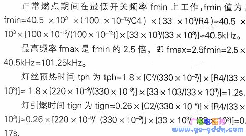
1. Startup and Oscillation: Upon power-on, the DC high voltage charges the external capacitor connected to the VDD pin via a startup resistor. Once the VDD voltage exceeds 13V, the IC starts oscillating. The internal voltage-controlled oscillator (VCO) generates a sawtooth waveform that determines the switching frequency. This frequency is influenced by the external capacitor CCF, resistor RIREF, and voltage on the CSW pin.
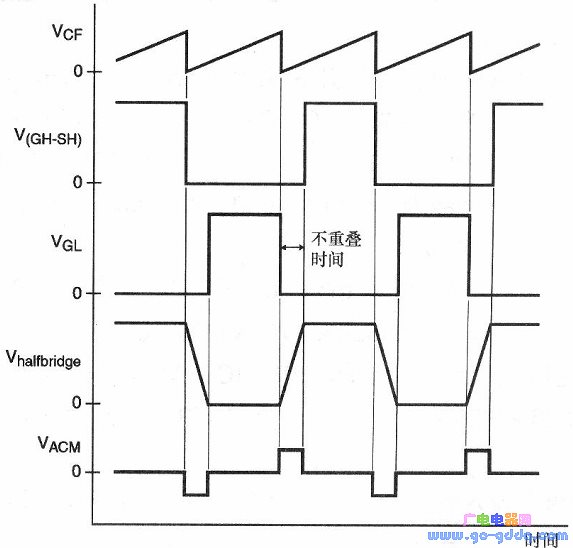
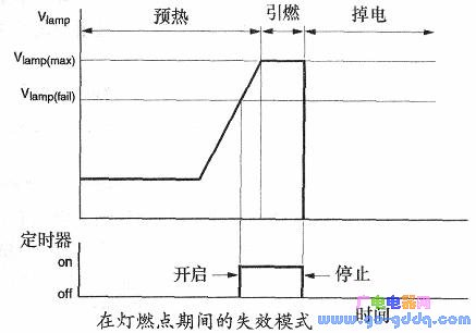
2. Timing Circuit: The timing circuit includes a clock generator and counter that manage the preheating and ignition phases. During preheating, the oscillator starts at the highest frequency and gradually decreases until the preheat voltage threshold is reached. This triggers the warm-up timer and adjusts the frequency accordingly.
3. Ignition: After preheating, the frequency is scanned to reach the load's resonant frequency, generating sufficient voltage to ignite the lamp. If the lamp fails to light, the circuit enters a protective shutdown mode.
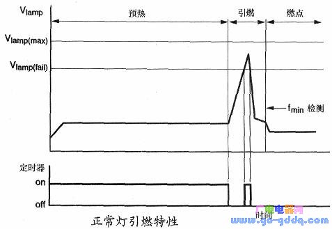
4. Lamp Failure Mode: The UBA2028 detects lamp failures during both ignition and operation. If the lamp voltage exceeds a set threshold, the circuit will stop oscillating and enter a safe state to prevent damage.
5. Capacitive Mode Protection: If the voltage on the ACM pin exceeds certain thresholds during the dead time, the circuit assumes a capacitive mode and increases the frequency to avoid hard switching, thus protecting the MOSFETs.
Application Circuit Example

The above circuit shows a 20W CFL electronic ballast using the UBA2028. It includes components such as a fuse resistor R1, EMI filter (C11, L1, C12), bridge rectifier D1, and charge pump circuit (D2, D16, Cin). The DC high voltage is applied to the HV pin, and the VDD pin is powered through resistors R3 and R12, along with a charge pump circuit.
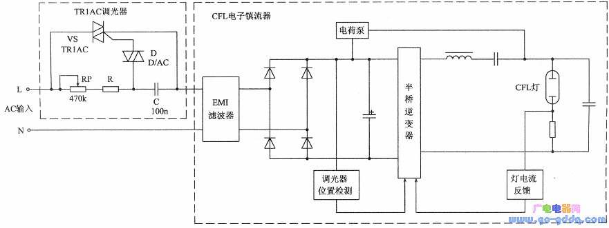
Dimming functionality can be achieved by connecting a triac dimmer to the input. A dimmer state detector circuit (R20, R9, R21, C28, D11, D8, R22, R13, R18, C29) feeds the detection signal into the CSP pin of the IC, allowing the UBA2028 to adjust the lamp brightness accordingly.
Solar tracker system,Fully automatic solar tracker,Solar tracker structure,Solar tracker bracket
Hebei Shuobiao New Energy Technology Co., Ltd. , https://www.pvbracketsystem.com