Supercapacitors [SC] or ultracapacitors, also known as electric double-layer capacitors, are increasingly used in a variety of power management systems. In automotive applications, such as start-stop systems with regenerative braking, the supercapacitor can provide the energy needed to engage the starter to restart the combustion engine and receive kinetic energy recovered during braking. The advantage of supercapacitors is that they charge and discharge significantly more times than traditional lead-acid batteries, while at the same time being able to absorb energy more quickly without reducing their life expectancy. These features also make supercapacitors attractive for industrial backup power systems, fast-charging cordless power tools, and remote sensors, as frequent replacements are impractical for these applications.
This article discusses the challenges of charging these large capacitors and shows power system design engineers how to evaluate and select the best system configuration for a backup energy storage application. An example of a supercapacitor charger solution is presented, along with waveforms and detailed explanations.
System details
Many system configurations use a supercapacitor bank as a backup energy storage component. In the beginning, the design engineer needs to determine its energy storage configuration goals and then decide how much voltage is available to store the energy. The choice of solution depends on the power and voltage requirements of the load, as well as the energy and voltage capabilities of the supercapacitor. Once the best solution has been determined, the overall performance and cost must also be balanced.
Figure 1 shows a block diagram of a high-efficiency solution where the load is a device that requires a stable input voltage (3.3V, 5V, 12V, etc.). The 48V mains supply powers the normally functioning switching regulator 2 (SW2) while charging the supercapacitor bank through switching regulator 1 (SW1) to a voltage of 25V. When the main power is disconnected, the supercapacitor bank supplies power to SW2 to maintain continuous operation of the load.
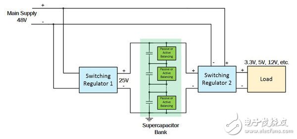
Figure 1. Block diagram of a battery backup system using a supercapacitor bank
After selecting the supercapacitor, the system engineer must also select the target voltage to charge the supercapacitor based on the rating curve of the supercapacitor. Most supercapacitor units are rated for 2.5V-3.3V at room temperature, and this rating drops at higher temperatures, which in turn leads to longer life expectancy. Generally, the charging target voltage setting value should be lower than the maximum rated voltage to extend the working life of the super capacitor.
Next you need to select the expected voltage and SW2 topology for the supercapacitor bank. The supercapacitor bank configuration can be a series capacitor series combination of parallel, series or parallel. Since the cell capacitor voltage rating is typically less than 3.3V and the load often requires equal or higher supply voltages, the option for capacitor cell configuration and SW2 is to use one capacitor cell with one boost converter, or multiple in series A capacitor unit with a buck or buck-boost regulator. If a boost configuration is used, we must ensure that the voltage does not drop below the minimum operating input voltage of SW2 when the supercapacitor is discharged. This voltage drop can be as much as half of the supercapacitor charging voltage. To this end, we give an example of a supercapacitor bank consisting of a series supercapacitor combination and a simple buck regulator (SW1). Then, if required by the energy requirements, multiple series capacitor strings will be connected in parallel.
If a series combination of supercapacitors is selected, the number of capacitor cells used must be selected based on the maximum expected voltage at the top of the capacitor string. More series capacitance means that the super capacitor string has a smaller capacitance value and a higher voltage. For example, suppose you choose to use two strings of capacitors consisting of four 2.7V10F capacitors and one capacitor string consisting of eight identical capacitors (in series). While the two configurations can store the same total charge and energy, the available voltage range of the capacitor string makes a single series string advantageous. For example, if there is a load that requires a 5V bias, then SW2 requires a voltage of around 6V (given its maximum duty cycle and other differential pressure factors).
â— Energy in the capacitor W = CV2/2, available energy W = C / 2 (Vcharge2 - Vdicharge2)
â— For two capacitor strings of 4 capacitors per string, the available energy W = 2*[(10F/4)/2*((2.7V*4)2-6V2)] = 201.6J
â— For a single capacitor string containing 8 capacitors (series), the available energy W = 1*[(10F/8)/2*((2.7V*8)2-6V2)] = 269.1J
Since the two capacitor banks can store the same total energy, the charge/disabling percentage of the lower voltage capacitor string is greater. In this case, a higher capacitor string voltage is preferred to take advantage of the supercapacitor.
The third system challenge comes from how to charge the supercapacitor bank. In the beginning, when the supercapacitor voltage is 0, due to the high capacitance value, SW1 needs to work for a long time under the condition of similar output short circuit. Regular SW1 may be stuck in hiccup mode and cannot charge the supercapacitor. To protect the supercapacitor and SW1, additional current limiting is required at the beginning of the charging phase. A satisfactory solution is to allow SW1 to provide a continuous charging current for a long period of time with almost no output voltage.
There are many ways to charge a super capacitor. Constant current/constant voltage (CICV) is the preferred method of choice, as shown in Figure 2 (CIVE curve). At the beginning of the charging cycle, the charging device (SW1) operates in a constant current mode, providing a constant current to the supercapacitor such that its voltage increases linearly. When the supercapacitor is charged to the target voltage, the constant voltage loop activates and accurately controls the supercapacitor charge level to keep it constant to avoid overcharging. Again, this prioritized solution also addresses the requirements for power management functions that need to be considered in the design.
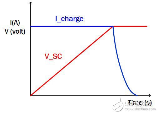
Figure 2. CICV Super Capacitor Charge Control
Taking Figure 1 as an example, in the case of a 48V main power supply, a 25V super capacitor bank voltage, and a load voltage of 3.3V, 5V, 12V, etc., it is suitable to select a synchronous buck function for SW1 and SW2. Since the main challenge is related to supercapacitor charging, the choice of SW1 is very important. The ideal solution for SW1 requires power management functions to operate at high input (48V) and output (25V) while providing CICV modulation.
Super Capacitor Charger Solution Example
To illustrate the supercapacitor charging behavior, we take the synchronous buck regulator as an example. Explain its key issues and solutions, and use experimental waveforms to help understand.
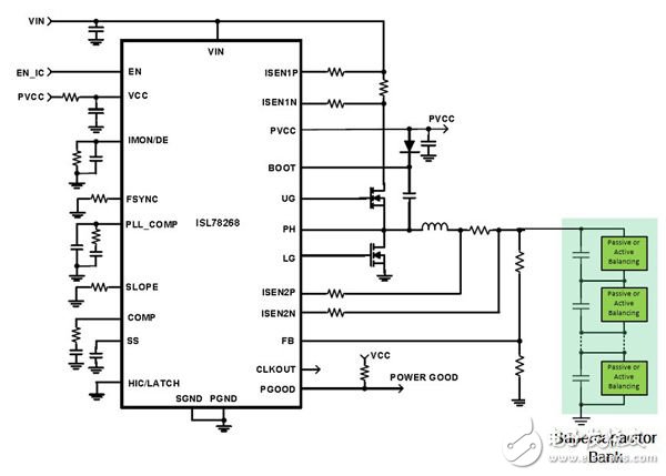
Figure 3. Simplified schematic of a synchronous buck regulator for CICV supercapacitor charge control
Figure 3 shows a simplified schematic of a synchronous buck regulator implementing CICV mode controlled by Intersil's ISL78268. In order to charge the supercapacitor bank to 25V under CICV control, the following functions were considered when selecting the controller:
1. Synchronous buck controller that can operate with VIN > 48V and VOUT > 25V.
2. Constant current and constant voltage adjustment capability, which can automatically switch the adjustment mode.
3. Implement accurate current sensing input in the system supply voltage range to achieve CI mode. Referring to Figure 3, the controller senses the continuous current of the inductor, i.e., the charging current. The controller's current sense amplifier must be able to withstand the common mode voltage, which is 25V in this example.

Figure 4 shows a small functional block diagram of the ISL78268 synchronous buck controller. As shown, there are two independent error amplifiers, labeled Gm1 and Gm2, for achieving a constant voltage (Gm1) and a constant current (Gm2).
The error amplifier Gm1 is used for CV closed loop control. It compares the feedback voltage of FB with the internal 1.6V reference voltage and produces an error voltage on the COMP pin. The FB pin is connected from the output voltage to a resistor divider and is set to a FB voltage of 1.6V when the output voltage is at the expected voltage level. The COMP voltage then represents the difference between the expected output voltage and the actual output voltage. The COMP is then compared to the inductor current to generate a PWM signal to control the output voltage to remain constant.
The error amplifier Gm2 is used for CI closed loop control. It compares the IMON/DE pin voltage to the internal 1.6V reference voltage and produces an error voltage on the COMP pin. The IMON/DE pin voltage is internally generated and represents the average output inductor current load value. Therefore, the COMP voltage is active when the Gm2 loop is active (the diode between the outputs of Gm1 and Gm2 effectively selects which loop is active) to represent the difference between the expected output current and the actual output current. The COMP is then compared to the inductor current to generate a PWM signal to control the output voltage to remain constant.
In the charging phase before the supercapacitor voltage reaches the target voltage, the COMP pin is driven by the output of Gm2 to generate a PWM output for CI control. When the supercapacitor voltage reaches the target value, the charging current decreases, causing the IMON/DE pin voltage to drop and the CI loop to be disconnected (when IMON/DE "1.6V), so the CV loop naturally takes over the control of COMP, thus Keep the output voltage constant.
The ISL78268 buck controller features both a peak current mode PWM controller (a reliable cycle-by-cycle peak current modulator) and an external constant average current loop that is ideal for supercapacitor charging.
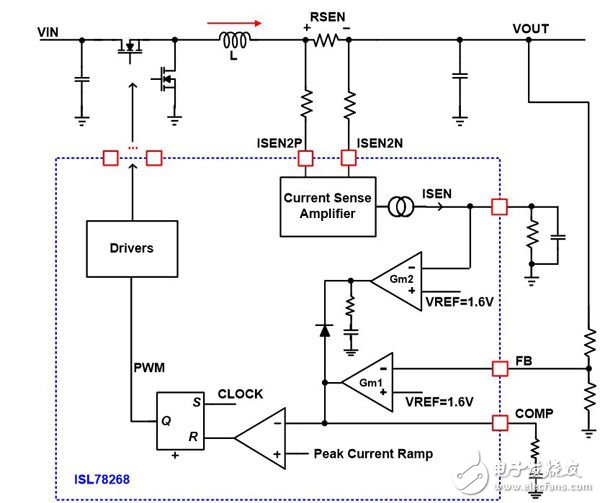
Figure 4. Simplified block diagram of the ISL78268 CICV loop
Now, we can focus on the implemented supercapacitor charging implementation. Figures 5, 6 and 7 show the experimental waveforms of a synchronous buck controller controlled by the ISL78268 to charge a supercapacitor bank (12-band 50F/2.7V series capacitor). The super capacitor will be charged to 25V from the mains.
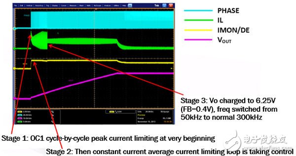
Figure 5. Experimental waveform of supercapacitor charging
Figure 5 shows that there are multiple stages in charging a supercapacitor. Initially, in the first phase, the average current signal on the IMON/DE pin of Vo is almost 0.ISL78268 has not reached 1.6V (the reference value of the expected charging current), so the CI loop has not yet been engaged. At this stage, the peak current of the inductor is limited cycle by cycle to a fixed OC threshold. At the beginning of the charging phase where VOUT is at a low level (FB "0.4V", the maximum switching frequency is limited to 50 kHz to prevent the mentioned inductor runaway problem due to the peak current limit at low VOUT.
Figure 6 shows an enlarged view of the waveform of the first stage. Phase 2 begins when the IMON/DE pin voltage (yellow trace) reaches 1.6V. At this stage, the CI loop turns on and pulls down the COMP signal (cyan trace) to begin stabilizing the output current and keeping the IMON/DE pin voltage constant. The IMON/DE pin voltage represents the sensed average output current signal. The IL waveform (green trace) shows that the average current is controlled to a constant level in phase 2. The output voltage waveform (pink trace) shows that the supercapacitor is charged linearly by a constant charging current.
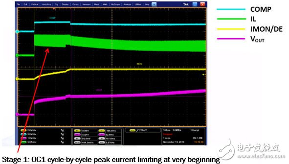
Figure 6. Experimental waveform amplification for stage 1 of supercapacitor charging
Phase 3 begins with a 0.4V voltage detected on the FB pin (Figure 7). After this trigger, the constant current stabilization loop will be fully turned on, so the switching frequency can be automatically adjusted to a pre-programmed 300kHz. At higher switching frequencies, the inductor current ripple (green trace) is significantly reduced. The output voltage (pink trace) continues to increase linearly, indicating that the supercapacitor is linearly charged.
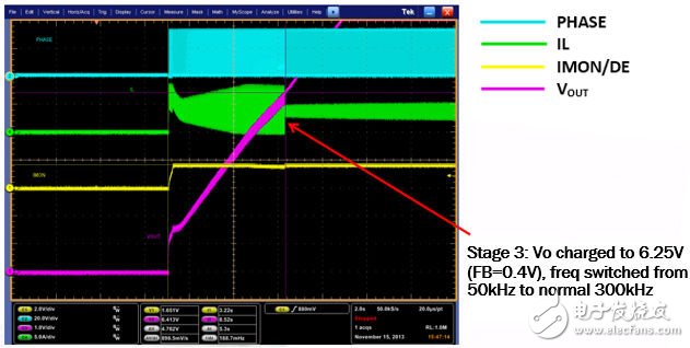
Figure 7. Experimental waveform of supercapacitor charging
Returning to Figure 5, the third stage ends when Vo reaches a target voltage of 25V. At this point, the CV loop is turned on and the output voltage is stabilized. The average current loop is broken. Figure 5 shows that the output voltage (pink trace) is flat and the inductor current is reduced. The IMON/DE pin current, which represents the average charging current, also drops, indicating the end of the constant current stabilization process.
Conclusion
Supercapacitors are used as energy storage solutions in automotive, industrial, and consumer products due to their inherent physical characteristics compared to traditional batteries. In order to maximize the storable energy of the supercapacitor bank, the best solution is often to connect multiple supercapacitor cells in series to achieve a high capacitance group voltage. When charging, it is best to use the CICV method to limit the high current generated by the low ESR during charging of the supercapacitor to a constant voltage. The constant current also allows the charge loss to be controlled, which reduces the amount of heat generated and extends the life of the supercapacitor. Therefore, it is beneficial to have the charging circuit tolerate high voltages and provide CICV control functions.
Security and protection system (SPS) security & protection system, in order to maintain social public safety, the use of security products and other related products constitutes an intrusion alarm system, video security monitoring system, access control system, BSV LCD video wall system, access control fire System, explosion-proof safety inspection system, etc.
Security mainly includes: closed-circuit monitoring system, anti-theft alarm system, building intercom system, parking plant management system, community card system, infrared perimeter alarm system, electronic fence, patrol system, attendance access control system, security room system, electronic examination room system , smart door locks, and more.
As technology continues to advance, the security industry continues to expand. Specialized services such as alarm operation, intermediary, and information began to take off; the product range has been continuously enriched, and it has developed into dozens of categories, such as video surveillance, entrance and exit control, intrusion alarm, explosion-proof security, and thousands of varieties; closed-circuit monitoring is developing rapidly.
Security Pcb,Security System Circuit Board ,Security Pcb Circuit Board,Security Printed Circuit Board
Chuangying Electronics Co.,Ltd , https://www.cwpcb.com