In high-speed HDI PCB design, via design plays a crucial role. A via consists of a hole, a surrounding pad area, and a power layer isolation region. It is typically categorized into three types: blind vias, buried vias, and through holes. During the PCB design process, analyzing the parasitic capacitance and inductance of vias helps engineers optimize high-speed PCB performance.
Today, high-speed PCBs are widely used in communication systems, computers, and image processing applications. These advanced electronic products require low power consumption, minimal electromagnetic radiation, high reliability, and compact designs. To meet these demands, via design becomes an essential consideration in high-speed PCB layout.
**1. Through Holes**
A through hole is a fundamental component in multi-layer PCBs. It is composed of three main parts: the drilled hole, the annular pad around the hole, and the power layer isolation area. The manufacturing process involves electroplating the inner walls of the hole to connect copper layers on different board levels. The top and bottom of the via are usually designed as regular pads, which can either directly connect to traces or remain isolated. Vias serve as electrical connections, helping to secure components and improve signal integrity.
The schematic of a via is shown in Figure 1.
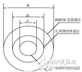
*Figure 1: Schematic diagram of vias*
Vias are generally divided into three categories: blind vias, buried vias, and through holes. Blind vias connect the outer layer to one or more inner layers but do not extend through the entire board. Buried vias are located entirely within the inner layers and do not reach the surface. Through holes, on the other hand, pass through all layers of the PCB and are commonly used for internal interconnections or component mounting.
The classification of vias is illustrated in Figure 2.
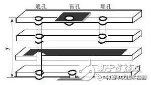
*Figure 2: Classification of vias*
**2. Parasitic Capacitance of Vias**
Each via has a parasitic capacitance to the ground plane. This capacitance can affect signal integrity by increasing the rise time of signals and reducing overall circuit speed. The formula for estimating the parasitic capacitance of a via is:
C = 1.41 × ε × T × D1 / (D2 - D1)
Where:
- ε is the dielectric constant of the board material
- T is the thickness of the PCB
- D1 is the diameter of the via pad
- D2 is the diameter of the via hole on the ground layer
Minimizing this capacitance is key to improving high-speed performance.
**3. Parasitic Inductance of Vias**
Parasitic inductance in vias can be more problematic than capacitance in high-speed digital circuits. It weakens the effectiveness of bypass capacitors and reduces the filtering capability of the power distribution system. The formula for estimating via inductance is:
L = 5.08 × h × [ln(4h/d) + 1]
Where:
- h is the length of the via
- d is the diameter of the via
From this equation, it's clear that the length of the via has a greater impact on inductance than its diameter.
**4. Non-Through Hole Technology**
Non-through hole technology includes blind and buried vias. These allow for smaller, lighter PCBs with fewer layers, better electromagnetic compatibility, and improved performance. They also reduce manufacturing costs and simplify routing, especially for high-density designs like BGA packages.
Using non-through holes reduces the number of large vias on the board, freeing up space for signal traces and shielding. This improves EMI/RFI performance and allows for better power and ground plane integrity. Additionally, non-through hole technology reduces the workload compared to traditional mechanical drilling methods.
**5. Via Selection in Standard PCBs**
In standard PCB designs, the impact of via parasitics is less significant. For 1–4 layer boards, common via sizes are 0.36mm (drill), 0.61mm (pad), and 1.02mm (power isolation). Special signals such as power, ground, and clock lines may use larger vias, like 0.41mm/0.81mm/1.32mm. Designers should choose based on actual requirements and board density.
**6. Via Design in High-Speed PCBs**
In high-speed PCB design, even small vias can have significant negative effects. To minimize these, consider the following:
1. **Choose appropriate via size**: For general multi-layer boards, 0.25mm/0.51mm/0.91mm (hole/pad/power isolation) is preferred. For high-density boards, 0.20mm/0.46mm/0.86mm may be used. Avoid using very small vias if possible.
2. **Increase the power isolation area**: Larger isolation areas help reduce coupling and improve signal integrity.
3. **Minimize via usage**: Reduce unnecessary vias to keep signal paths short and clean.
4. **Use thinner PCBs**: Thinner boards help reduce both parasitic capacitance and inductance.
5. **Place power and ground pins close to vias**: Shorter leads reduce inductance, while thicker traces lower impedance.
6. **Add ground vias near signal vias**: This provides a low-inductance return path for high-speed signals.
While smaller vias offer advantages in high-speed design, they also increase manufacturing complexity and cost. Balancing performance, cost, and manufacturability is critical in high-speed PCB design.
**Choose high-speed PCB design, and unlock a promising, high-paying career in the future!**
>> Learn more about the course
MPPT Solar Charge Controller
MPPT (Maximum Power Point Tracking) solar charge controllers are an essential component in solar power systems. They are used to regulate the charging process and maximize the efficiency of solar panels. By continuously tracking the maximum power point (MPP) of the solar array, MPPT charge controllers ensure that the maximum available power is extracted from the solar panels and delivered to the Battery bank.
MPPT charge controllers with built-in inverters are designed for off-grid solar power systems. In addition to regulating the charging process, they also convert the DC power from the solar panels into AC power that can be used to power household appliances. These charge controllers are commonly used in remote locations where grid power is not available.
MPPT charge controllers with built-in load control are designed to regulate the charging process and control the power output to a specific load. They are commonly used in applications where the solar power is directly used to power specific devices or equipment. They play a crucial role in maximizing the efficiency of solar power systems by continuously tracking the maximum power point of the solar array. Whether it is a standalone controller, a controller with built-in inverters, or a controller with built-in load control, MPPT charge controllers are essential for efficient solar power utilization.
MPPT Solar Charge Controller Inverter,Mppt Charge Controller,Off-Grid Storage Controller,Mppt Solar Controller
Bosin Power Limited , https://www.bosinsolar.com