1 Introduction
This article refers to the address: http://
A typical GPS receiver consists of four main components: an antenna, an RF front end, a correlator, and a navigation solver. In order to ensure real-time processing of the GPS receiver, the key baseband signal processing module-correlator is generally implemented by an application specific integrated circuit. For software GPS receivers, the RF front-end module is still implemented by hardware, and the baseband processing is implemented by software. The software platform can be a digital signal processor (DSP) or a general-purpose PC. It is an active direction for the development of GPS receivers to collect real GPS signals and store them on the hard disk of ordinary PCs. The software receivers are designed and developed by using PC's rich hardware and software resources. In order to ensure the validity of GPS data collection, the indicators to be comprehensively considered include sampling rate, number of quantization bits, and continuous integrity of data. This is the basis for selecting a data acquisition system.
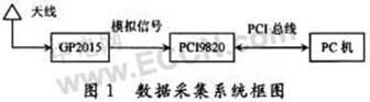
This article describes a PCI-based approach. The data acquisition system of the bus uses the PCI9820 data acquisition card produced by ADLINK to realize the acquisition of the IF GPS data output by the ZARLINK RF module GP2015, and the data is stored on the hard disk for subsequent GPS baseband signal processing and positioning solution work. . The block diagram of the data acquisition and processing system is shown in Figure 1.
2 PCI9820 data acquisition card introduction
The PCI9820 is a high-speed, high-resolution, high-capacity PCI bus data acquisition card with two analog inputs for simultaneous acquisition. It provides an internal clock reference of 60 MHz. Under the internal clock reference, when the two sets of analog inputs work simultaneously, the maximum sampling rate is 60 MS/s, while the external clock reference can reach 65 MS/s; when one analog input is selected If the "ping-pong" mode is enabled, the internal time base sampling rate is up to 120 MS/s, and the external time base sampling rate can reach 130 MS/s.
The PCI9820 has a resolution of 14 b, and the A/D resolution of 14 b makes the PCI9820 ideal for both time domain and frequency domain applications. The range of input can be selected by software and provides a range of -1 to 1 V or -5 to 5 V. The input impedance can be provided by two jumpers, J6 and J7 on the back of the board, for 50 Ω and 1 MΩ.
The PCI9820 offers a variety of trigger options, including software triggering, analog triggering, and digital triggering. The analog trigger function provides a choice of multiple trigger conditions, while the digital trigger provides both a rising edge trigger and a falling edge trigger. The available trigger modes are post-trigger, pre-trigger, delayed trigger, and intermediate trigger. For continuous trigger events with very short intervals, data can be acquired in repeated trigger mode. When applying multi-card synchronization, the PCI9820 can accept 5 V/TFL digital trigger signals from SSI VIs and external SMB interfaces, and multi-cards share clocks and trigger signals.
PCI9820 continues the design of ADLINK on the DAQ-2000 series, providing automatic correction function. The user can activate the automatic correction function on the PCI9820 through a software command to complete the calibration of the analog input channel without any complicated manual operations. .
The PCI9820 uses standard SODIMMSDRAM for data storage in digital design. Because the data stream generated by the single channel of PCI9820 has exceeded the bandwidth of 33 MHz and 32 b PCI bus, the data is recorded in the onboard SDRAM before being transferred to the computer, and then transferred to the host memory through the bus control DMA. in. When the speed of data exceeds the PCI bus bandwidth, the memory capacity on the board is relatively important. The standard version of the PCI9820 comes with 64 MB of memory and supports up to 512 MB, providing up to several seconds of storage for a single channel acquisition rate of 130 MS/s. If the data output of the board is less than the PCI bandwidth, the PCI9820 can be configured with an onboard 3k sample FIFO bypass SDRAM to complete real-time data transfer to the host memory. In a multi-user or multi-tasking operating system, it is difficult to allocate a large contiguous memory for DMA transfer, so the PCI9820 provides a scatter DMA function that can connect discrete memory blocks into one interconnect. Table columns, so that large-capacity data transmission can be realized without being affected by the scattered small-capacity memory blocks. Its structural block diagram is shown in Figure 2.

3 GPS RF chip GP2015 introduction
GP2015 is a small RF front-end chip in the TQFP package produced by ZARLINK. GP2015 provides a low-power, low-cost and high-reliability GPS RF front-end solution. The GP2015 includes an on-chip synthesizer, mixer, automatic gain control (AGC), and a quantizer that provides symbol and magnitude digital outputs to form a complete GPS receiver. The RF front-end circuitry requires very few external components. It can be used with GPS baseband processors such as the 12-channel GPS correlator GP2021 or GP4020, suitable for satellite receivers, time standards, navigation and measurement applications for C/A code global positioning.
The RF front end is mainly composed of GP2015 chip and peripheral filter circuit. The input signal of GP2015 is the first local oscillator signal (1.4 GHz) generated by the preamplifier filtered and amplified GPS signal (L1 band is 1 575.42 MHz) as input signal and phase-locked loop frequency synthesizer. Mixing, filtering to get the difference frequency signal (175.42 MHz). This signal is mixed with the second local oscillator signal (140 MHz) and selected by the center frequency of the SAW filter to obtain the difference frequency signal (35.42 MItz). This signal then enters the IF signal main amplifier, which consists of two AGC (Automatic Gain Control) amplifiers and a three-stage inverter. The signal is first amplified by AGC and then mixed with the third local oscillator signal (31.11 MHz) and the intermediate frequency signal (4.309 MHz) is selected via a low pass filter. The IF signal is sent all the way to the on-chip A/D converter and sent to pin 1 for testing.
After the IF signal is subsequently input into the A/D converter for 2 b quantization, the analog signal is converted into a two-bit digital signal - symbol and mode (SIGN and MAG), which represent the polarity and amplitude values ​​of the output signal, respectively. The comparison result from the real-time output of the intermediate frequency analog signal after comparison by the comparator. The output of the comparison result is locked by the clock signal (5.714 Mttz) provided by the baseband correlator, which locks the 4.309 MHz signal to the 1.405 MHz digital signal. The digital signal is output to the baseband processor for further processing.
Here, the analog intermediate frequency signal of 4.309 MHz of the first pin of GP2015 is sent to the PCI9820 data acquisition card, and the digital intermediate frequency GPS signal is collected according to a certain sampling rate.
The RF module built with GP2015 also includes the design of the peripheral filter. The function of the RF filter is to filter out the out-of-band interference, especially the image noise of 1 224.58 MHz, to avoid overloading the RF front-end mixer. The filter also helps to filter out interference from 900 MHz mobile phones. The insertion loss introduced by the RF filter needs to be compensated by the LNA pre-low noise amplifier. Specific details can be found in the manual and literature [5-7].
4 sampling scheme and signal spectrum analysis
4.1 Sampling plan
The GP2015 outputs an analog IF signal of 4.309 MHz, while the C/A code bandwidth of the GPS is 2.046 MHz. Therefore, the frequency band of the GPS signal is 3.286 to 5.332 MHz, and the highest frequency of the IF signal is fH=5.332 MHz. According to the Nyquist low-pass sampling theorem, when the sampling frequency fs≥2fH, the original signal can be recovered from the sampled data without distortion, and the sampling of the signal in the time domain is equivalent to the periodic extension in the frequency domain, so that Fs ≥ 2fH is to ensure that the spectrum of the signal after sampling does not overlap, so the sampling frequency is at least fs=10.664 MHz. However, the higher the sampling frequency, the greater the amount of data processed by the back-end digital baseband processing, which makes it difficult to process GPS signals in real time. Therefore, the bandpass sampling technique is often used in engineering practice to reduce the sampling rate, which is beneficial to simplifying hardware, reducing costs, and reducing the pressure of subsequent data processing.
For the band-pass signal in GPS, the bandwidth is B=2.046 MHz. As long as some values ​​of fs≥2B are taken, it can ensure that the spectrum of the signal after sampling does not overlap. This sampling method is called Band-Sampling, also called Under-Sampling. The band-pass sampling frequency fs can be determined by the following formula:
![]()
Where fH is the highest frequency of the bandpass signal, fL is the lowest frequency of the bandpass signal, n is an integer, and the value ranges from 2≤n≤fH/(fH-fL).
For the GPS IF signal here, fH=5.332 MHz, fL=3.286 MHz, obtained by equation (1):
![]()
When n=2, fs range: 5.332 MHz ≤ fs ≤ 6.572 MHz, so in engineering practice, the baseband chip GP2021 (GP4020) with GP2015 provides a sampling clock frequency of 5.714 MHz, and undersampling yields a digital intermediate frequency of 1.405 MHz. signal.
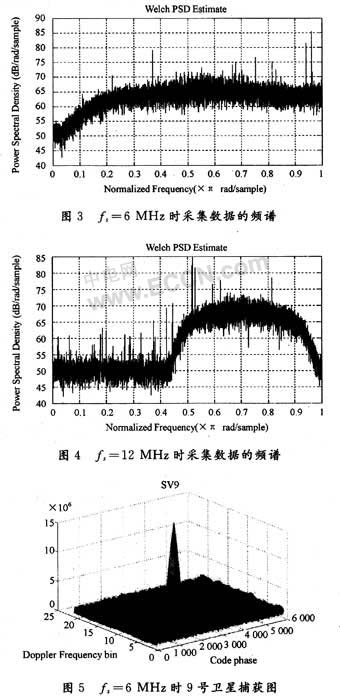
The internal clock reference of the PCI9820 capture card is 60 MHz. It can be set in the software to divide the integer ratio, that is, fs=60/n, n is an integer. Let us take n=10 and get the sampling frequency fs=6 MHz. According to this frequency, the GPS intermediate frequency signal is sampled to obtain a digital intermediate frequency signal of 1.691 MHz. The experiment was also carried out using a low-pass sampling frequency fs=12 MHz.
4.2 PCI9820 double buffer data acquisition mode
In a DOS environment, data collected by one DMA or interrupt mode usually cannot exceed 640 kB. In the Windows environment, the amount of data in a DMA depends on the addressing range of the PCI controller chip of the board and the physical memory size of the system. Although it may be large, it still cannot realize long-time real-time data acquisition, and the double buffer provided by the PCI9820. The pattern can solve this problem.
Double buffering is a circular buffer, and one is a user buffer. The circular buffer is divided into two parts. The acquired data is first written to the circular buffer. When half full, the first half of the circular buffer is written to the user buffer. The acquired data continues to be written to the second half of the circular buffer. When the circular buffer is full, the second half of the circular buffer is written to the user buffer. At this point, the collected data continues to be written to the first half of the circular buffer. Repeatedly, once every half is full, the front or back half of the circular buffer will be written to the user buffer to achieve continuous high-speed acquisition. It is worth noting that the double buffering method involves frequent reading and writing of the memory, so when the sampling rate is high or the system task is very busy, data loss may occur. Specific programming can refer to routines and literature [3, 4].
4.3 Sampling signal analysis
According to the sampling frequency scheme introduced above and the double buffered data acquisition mode of PCI9820, we collect the IF signal of GP2015, the data is stored on the computer hard disk, and the time-frequency analysis of these data is performed under the Matlab software platform, and the capture tracking process is performed.
The results show that when the sampling frequency is 6 MHz and 12 MHz, the data is continuous and reliable, providing real and reliable data for subsequent software baseband processing. Figure 3 and Figure 4 show the spectrum of the signal with the sampling frequency of 6 MHz and 12 MHz respectively. Figure 5 shows the data acquisition of the data sampled at 6 MHz, and the captured result of the satellite No. 9 shows that the data is in good condition.
5 Conclusion
The GPS data acquisition system constructed by PCI9820 high-performance data acquisition card and GP2015 RF module is used to realize continuous acquisition of GPS signals for a long time, and the data is analyzed and processed. The results show that the data is continuous and can be used for subsequent baseband processing. The software GPS receiver is realized, which also provides a reference for the collection and processing of other bandpass signals.
LSZH cables is the abbreviation term of (low smoke halogen free) low smoke zero halogen electrical cables.FR is for flame retardant power cables, also for the short term of Fire Resistant Power Cables. The smoke released by these cables is non-toxic when fire happens. Therefore they are applicable for public places to protect instruments, equipments and people from potential harm.Fire resistant Power Cable will still keep the electrical power on within certain time in case of combustion.Flame retardant power cable may produce low gases and smoke after combustion.These cables are generally used in population-concentrated public places to have better fire safety and rescue capability.
Specification
Conductor:99.99% oxygen free copper or aluminum
Insulation/Sheath: LSZH FR formula added
Rated Voltage:≤35KV
Packaging: wooden steel drum, wooden/paper/plastic reels


Main advantage
l Low or no halogen acid gas release
l Excellent resistance to weather (-30℃ to 105℃)and fire
l Withstanding high voltage and current stressing
l Good elasticity and stickiness, long life time
Application
l High-rise building
l Hospital , Large-scale library,Gym ,Hotel
l Bus station or railway station, Airport , passenger waiting room
l Cultural heritage building, nuclear power plant,important military facilities
l Subway ,underground shopping mall
Classification
The application of LSZH power cables are classified into 4 level based on using features, fire risk and difficult for evacuation and life-saving.
|
Application |
Flame Retardant Class Choice |
|
Superior |
Class A |
|
Grade 1 |
Class B |
|
Grade 2 |
Class C |
FAQ
Q: Are you a factory or trading company?
A : We are a manufacturer. We are professional in
developing and producing electrical wires and cables since 2001.
Q: Can I visit your factory?
A :Yes! You are welcome to visit our factory for further detail check.
Our factory is located in Minqing,Fujian.You could choose to fly to Xiamen/Fuzhou International airport. And tell us your flight No. We will arrange to pick you up if you like.
Q: May I buy samples from you?
A: Yes! You are welcome to place sample order to test our superior quality and services.
Q: Can you put my brand name (logo) on these products?
A: Yes! Our factory accepts to print your logo on the products.
Q: May I know the status of my order?
A: Yes .The order information and photos at different production stage of your order will be sent to you and the information will be updated in time.
Please welcome to get in touch with us for further information about catalogue, production and price list. Will response as soon as possible. OEM service is available based on legal authorization. And you are also very welcome to visit our factory by mutual schedule check accordingly.
LSZH FR Power Cable,Lszh Fr Sheath Power Cable,Power Station Control Cable,Low Smoke Control Cables
Fujian Lien Technology Co.,Ltd , http://www.liencable.com