Many of the special features of RF circuits are difficult to describe in a few short sentences, nor can they be analyzed using traditional simulation software such as SPICE. However, there are currently some EDA software on the market with harmonic balance and shooTIng method. Such complex algorithms can quickly and accurately simulate RF circuits. But before learning these EDA software, you must understand the characteristics of the RF circuit, especially the meaning of some proper nouns and physical phenomena, because this is the basic knowledge of RF engineering.
RF interface
Wireless transmitters and receivers are conceptually divided into two parts: the fundamental frequency and the radio frequency. The fundamental frequency includes the frequency range of the transmitter's input signal and also the frequency range of the receiver's output signal. The bandwidth of the fundamental frequency determines the basic rate at which data can flow through the system. The fundamental frequency is used to improve the reliability of the data stream and to reduce the load imposed by the transmitter on the transmission medium below a particular data transmission rate. Therefore, when designing a baseband circuit for a PCB, a large amount of signal processing engineering knowledge is required. The transmitter's RF circuit converts and upconverts the processed baseband signal to a specified channel and injects this signal into the transmission medium. Conversely, the receiver's RF circuit can take signals from the transmission medium and convert and down-convert to the base frequency.
The transmitter has two main PCB design goals: the first is that they must emit as much power as possible while consuming the least amount of power. The second is that they cannot interfere with the normal operation of the transceivers in adjacent channels. As far as the receiver is concerned, there are three main PCB design goals: first, they must accurately restore small signals; second, they must be able to remove interfering signals outside the desired channel; the last point, like the transmitter, they must consume the power Very small.
Small expectation signal
The receiver must be sensitive to detect small input signals. In general, the receiver's input power can be as small as 1 μV. The sensitivity of the receiver is limited by the noise generated by its input circuitry. Therefore, noise is an important consideration when designing a receiver for a PCB. Moreover, the ability to predict noise with simulation tools is indispensable. Figure 1 is a typical superheterodyne receiver. The received signal is filtered first, and then the input signal is amplified by a low noise amplifier (LNA). This signal is then mixed with this signal using the first local oscillator (LO) to convert this signal to an intermediate frequency (IF). The noise performance of the front-end circuitry is primarily dependent on the LNA, mixer, and LO. Although traditional SPICE noise analysis can be used to find the noise of the LNA, it is useless for the mixer and LO because the noise in these blocks is severely affected by the large LO signal.
A small input signal requires the receiver to have a very large amplification function, which typically requires a gain of 120 dB. At such high gains, any signal that is coupled back to the input from the output can cause problems. An important reason for using a superheterodyne receiver architecture is that it distributes the gain across several frequencies to reduce the probability of coupling. This also makes the frequency of the first LO different from the frequency of the input signal, which can prevent large interference signals from "contaminating" to small input signals.
For some different reasons, in some wireless communication systems, a direct conversion or homodyne architecture can replace the superheterodyne architecture. In this architecture, the RF input signal is directly converted to the fundamental frequency in a single step. Therefore, most of the gain is in the fundamental frequency, and the LO is the same frequency as the input signal. In this case, you must understand the influence of a small amount of coupling, and you must establish a detailed model of the "stray signal path", such as: coupling through the substrate, package pins and bond wires. Coupling between (bondwire) and coupling through the power line.
Large interference signal
The receiver must be sensitive to small signals, even when large interfering signals (barriers) are present. This occurs when an attempt is made to receive a weak or long-range transmit signal, with a powerful transmitter nearby broadcasting in an adjacent channel. The interference signal may be 60~70 dB larger than the expected signal, and can block the reception of the normal signal by a large amount of coverage during the input phase of the receiver or by causing the receiver to generate excessive noise during the input phase. If the receiver is in the input phase and the interferer drives the non-linear region, the above two problems will occur. To avoid these problems, the front end of the receiver must be very linear.
Therefore, "linear" is also an important consideration when designing a receiver for a PCB. Since the receiver is a narrowband circuit, the non-linearity is measured by measuring "intermodula-TIon distorTIon". This involves using two sine or cosine waves of similar frequency and located in the center band to drive the input signal and then measure the product of its intermodulation. In general, SPICE is a time-consuming and costly simulation software because it has to perform many loop operations to get the required frequency resolution to understand the distortion.
Adjacent channel interference
Distortion also plays an important role in the transmitter. The non-linearity produced by the transmitter in the output circuit may spread the bandwidth of the transmitted signal in adjacent channels. This phenomenon is called "spectral regrowth." Before the signal reaches the transmitter's power amplifier (PA), its bandwidth is limited; however, the "interchanging distortion" in the PA causes the bandwidth to increase again. If the bandwidth is increased too much, the transmitter will not be able to meet the power requirements of its neighboring channels. When transmitting a digital modulation signal, in fact, SPICE cannot be used to predict the re-growth of the spectrum. Since approximately 1000 digital symbol transfer operations must be simulated to obtain a representative spectrum and also need to be combined with high frequency carriers, these will make SPICE transient analysis impractical.
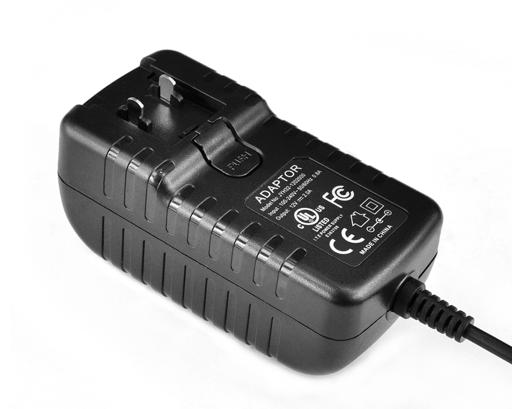
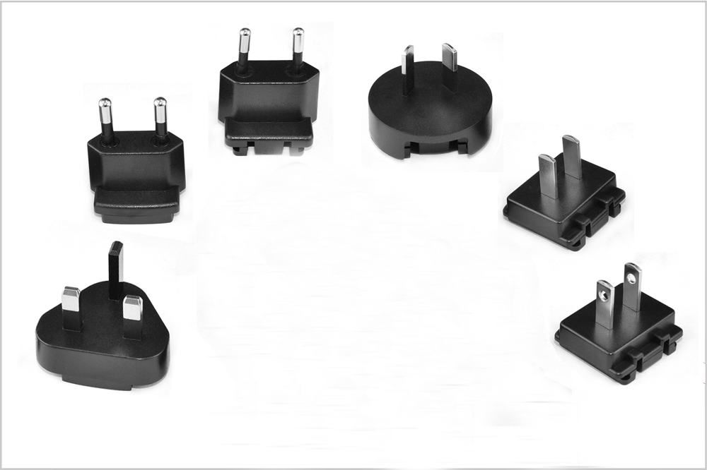
22V Plug in wall charger with interchangeable plugs was wildly used for tablet, bluetooth speaker, massage chair, humidifier, juice extractor, coffee machine, small household appliance, fingerprint scanner, CCTV camera-etc. For this 22V detachable plug power adapter, there are 6 different plugs types –Chinese plug, US plug, European Union plug, Korea plug, Australia plug and UK plug,you can only take one 22V plug in wall power adapter with you when you traveling among these 6 countries/regions. And we can also make more plugs if you tell us your specific requirement.
All our 22V wall mount Detachable Plug Power Adapter were get through 100% full-load burning test for at least 2 hours, and 3000Vac withstanding voltage test for 1 minutes.


22V Detachable Plug Power Adapter
22V Detachable Plug Power Adapter,Ul Detachable Plug Power Adaptor, 22V Adapter For Detachable Plug Power
Shenzhen Juyuanhai Electronic Co., Ltd. , https://www.powersupplycn.com