Traditional digital filters are typically implemented using application-specific integrated circuits (ASICs) or digital signal processors (DSPs). However, with the advancement of FPGA technology, a new approach has emerged. FPGAs use SRAM-based look-up tables (LUTs), which are highly efficient for parallel processing tasks. Compared to conventional methods, this architecture offers better scalability and parallelism, making it a popular choice for building high-performance, programmable filter systems.
One key technique used in FPGA-based filter design is the distributed algorithm, which is well-suited for implementing multiply-add operations. Since FPGAs lack dedicated multipliers, direct multiplication can be resource-intensive. To overcome this, lookup tables are used to store precomputed values, reducing the need for complex multiplications. This approach is particularly effective in designing low-pass FIR filters, where the symmetry of linear-phase filters helps minimize hardware requirements.
The distributed algorithm allows for efficient implementation by breaking down the filter’s computation into smaller, manageable parts. By utilizing memory resources instead of multipliers, the design becomes more flexible and scalable. Additionally, combining the distributed algorithm with pipeline techniques significantly improves the filter's speed, making it ideal for real-time applications.
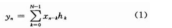
1 Distributed Filter AlgorithmA key characteristic of FIR filters is that their unit sample response h(n) has only a finite number of non-zero values. For an N-order FIR filter, the output y(n) is given by:
In many digital signal processing applications, traditional multiplication is not always necessary. Instead, the system function h(n) can be designed using tools like MATLAB’s fdatool, allowing the product terms to be treated as constants. Two common types of distributed algorithms are those for unsigned and signed numbers, both of which are widely used in FPGA-based FIR filter designs.
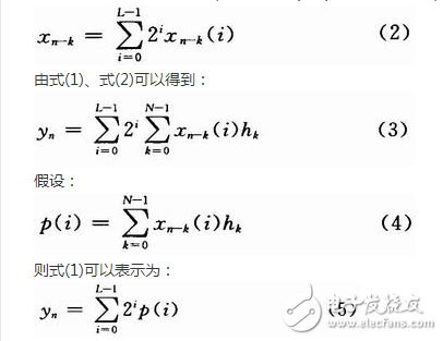
1.1 Distributed Algorithm for Unsigned NumbersGiven the parallel nature of FPGAs, if the input data x(n−k) has L bits, equation (1) can be restructured to take advantage of the FPGA’s parallelism. This allows for efficient computation through the use of precomputed values stored in lookup tables.
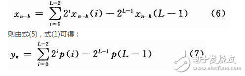
When dealing with signed numbers, the two’s complement representation is often used. This allows for efficient handling of negative values within the distributed algorithm framework.
Implementing a distributed algorithm for an N-term product-sum operation requires careful management of partial products. In FPGAs, this is achieved by preloading lookup tables with the necessary values. However, the size of the lookup table grows exponentially with the order of the filter, which can lead to high memory usage and performance issues.
To address this, large lookup tables can be split into smaller ones. For example, an 8th-order FIR filter can be divided into two 4th-order filters, significantly reducing the required memory and improving efficiency. This approach also makes it easier to scale the design for higher-order filters.
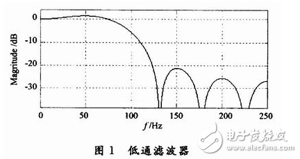
The system function for the filter is generated using MATLAB’s fdatool, with a sampling frequency of 500 kHz and a passband of 100 Hz. The resulting low-pass filter is shown in Figure 1. Similar designs can be adapted for high-pass or band-pass filters by changing the filter coefficients accordingly.
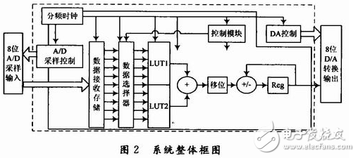
The system is implemented using Verilog HDL, and consists of four main components: the top-level file, A/D sampling, algorithm implementation, and D/A conversion. The overall system architecture is illustrated in Figure 2.
With an FPGA clock frequency of 100 MHz, the DAC0809 must operate at less than 1 MHz. Therefore, the system clock is divided by 200 in the top-level module to provide the appropriate clock for peripheral devices. Each module is then instantiated to form the complete system.
The A/D sampling process involves providing a 3-bit address, setting ALE to 1, and storing the address in a latch. This address is decoded to select one of the eight analog inputs. The START signal initiates the conversion, and the EOC signal indicates when the conversion is complete. Once the result is stored, it can be read via the OE signal.
The algorithm body includes several key components: data reception and storage, a data selector, two memory blocks, and an adder with control logic. These elements work together to process the incoming signals efficiently and produce the desired output.
48V20Ah Lithium Ion Battery,48V 20Ah Lithium Iron Electric Bicycle Battery,48V20Ah Electrict Scooter Battery,Lifepo4 Lithium Battery 48V20A
Jiangsu Zhitai New Energy Technology Co.,Ltd , https://www.zttall.com