A radio transceiver circuit using CMX017 / 018 single-chip UHFFM / FSK transmitter chip and receiver chip is introduced.
Keywords: UHF, FM / FSK, radio transmitter, radio receiver
1 Introduction The UHFFM / FSK radio transceiver circuit designed by the radio consists of two parts: radio transmission and reception. It can work in the UHF band (860 MHz to 965 MHz). It transmits and receives audio FM and digital FSK signals. The data transmission rate can reach 500 kbps, suitable Applications such as analog and digital narrowband, spread spectrum radio links, cordless phones, handheld data terminals, wireless local area networks, etc.
2 Circuit composition and working principle The radio transmission and reception circuits are respectively composed of UHFFM / FSK radio transmission chip CM017 and reception chip CM018 of CML (Consumer Microcircuits Limited) company. CM017 and CM018 IC are packaged in 28-pin SSOP and work in UHF frequency band. Operating voltage is 2.7 ~ 3.3V, with a power-saving sleep mode (10μA). When transmitting, the audio / digital signal to be transmitted is input from the CN017 modulation input terminal (MODIN), processed by the internal circuit of the CM017 chip, and then transmitted as an audio FM / digital FSK signal, and the transmission power can reach 100mW (+ 20dB). The transmitted signal can be received by the radio receiving circuit composed of CM018, processed by the internal circuit of the CM 018 chip, restored to audio / digital signal, and realizing the transmission of radio audio / digital signal.
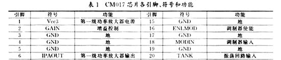
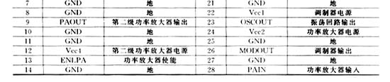
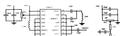
2.1 Transmitting circuit The radio transmitting circuit is composed of CM017 IC and some external resistance, capacitance and inductance coils. The circuit is shown in Figure 1. The CM017 chip includes FM / FSK modulator, 2-stage power amplifier, gain control and other circuits. As long as a few additional components are added to form a complete FM / FSK radio transmitter. Table 1 shows the pins, symbols and functions of the CM017 chip.
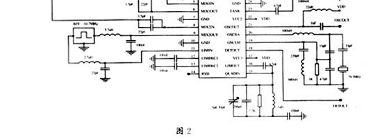
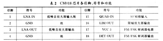
2. 2 receiving circuit The radio receiving circuit is made up of CM018 IC and some external resistance, capacitance and inductance coil, the circuit is shown in Figure 2. CM018 chip includes low noise amplifier (LNA), mixer (MIXER1, 2), voltage controlled oscillator (VCO), limiting amplifier (LIMI TE R) and FM / FSK demodulator and other circuits, only a few external The component can constitute a complete FM / FSK radio receiver. The pins, symbols and functions of the CM018 chip are shown in Table 2.

3 Regulation and control
3.1 Frequency control The potentiometer RV2 in the transmitting circuit and the potentiometer RV1 in the receiving circuit can control the RF operating frequency. The potentiometer control voltage varies from 0 to 3V, allowing the RF operating frequency to be set between 860 and 935MHz.
3.2 Gain control The potentiometer RV1 in the transmitter circuit controls the gain of the CMX017 power amplifier driver. When the GAIN terminal of the CMX017 is connected to 3V, the output power is maximum; when the GAIN terminal is connected to 0V, the gain is reduced by 20 dBm.
In the receiving circuit, the gain of the low noise amplifier (LNA) of the CMX018 is controlled by the switch SW2. When the switch is off, the LNA is in high gain mode, and when the switch is on, the LNA is in low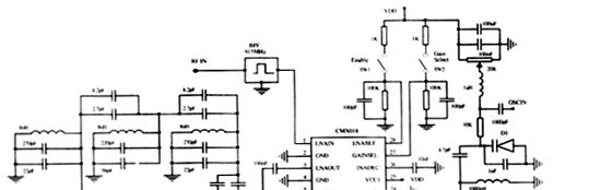
Gain mode (reduced from 16dBm to -6dBm).
3.3 Enable mode In the transmitting circuit, when the switches SW1 and SW2 are off, the CMX017 is in "sleep mode", and the chip current consumption is only 10 μA; when the switch SW1 is off and the switch SW2 is on, the CMX017 chip is in "Transmission standby mode", the power amplifier and power driver are in "low power consumption mode", the modulator and oscillator are in working state, and the current consumption is 24mA; when both SW1 and SW2 are turned on, the CM X017 chip is in "transmission mode" The circuit is in the transmitting state and the current consumption is 130mA. In the receiving circuit, when the switch SW1 is off, the CMX018 is in "sleep mode", the chip current consumption is only 10μA, when the switch SW1 is on, the chip is in "receiving mode", the circuit is in the receiving state, the current consumption is 50mA.
4 Printed circuit board design The printed circuit board design (PCB) of the transmitter and receiver circuits uses a 4-layer PCB. The top layer contains adjustment circuit connections, RF signal introduction and chip grounding; the second layer is a simple power ground board; the third layer Contains power connections for analog power supplies and additional circuits fed to all boards; the bottom layer contains grounds designed for shielding purposes. The microstrip technology is used in the design to provide a 50Ω line impedance on the PCB for the PAOUT and PAIN / MODOUT terminals of the transmitting circuit and the RFIN terminal of the receiving circuit.
5 Conclusion The experiment shows that the UHFFM / FSK radio transceiver circuit composed of CMX017 and CMX018 chips has a simple structure, easy debugging, stable and reliable performance, and can be widely used in wireless transmission and reception of audio FM or digital FSK signals. In the transmission and reception of digital signals, the use of single-chip microcomputer for data packaging, error correction, error detection, frequency hopping, and frequency, gain adjustment and mode control, can make the circuit adapt to more applications.
2 Consumer Microcircuits Limited. EV0181 EvaluaTIonKit User Manual. Consumer Micro cir cuits Limited, 2001
Keywords: UHF, FM / FSK, radio transmitter, radio receiver
1 Introduction The UHFFM / FSK radio transceiver circuit designed by the radio consists of two parts: radio transmission and reception. It can work in the UHF band (860 MHz to 965 MHz). It transmits and receives audio FM and digital FSK signals. The data transmission rate can reach 500 kbps, suitable Applications such as analog and digital narrowband, spread spectrum radio links, cordless phones, handheld data terminals, wireless local area networks, etc.
2 Circuit composition and working principle The radio transmission and reception circuits are respectively composed of UHFFM / FSK radio transmission chip CM017 and reception chip CM018 of CML (Consumer Microcircuits Limited) company. CM017 and CM018 IC are packaged in 28-pin SSOP and work in UHF frequency band. Operating voltage is 2.7 ~ 3.3V, with a power-saving sleep mode (10μA). When transmitting, the audio / digital signal to be transmitted is input from the CN017 modulation input terminal (MODIN), processed by the internal circuit of the CM017 chip, and then transmitted as an audio FM / digital FSK signal, and the transmission power can reach 100mW (+ 20dB). The transmitted signal can be received by the radio receiving circuit composed of CM018, processed by the internal circuit of the CM 018 chip, restored to audio / digital signal, and realizing the transmission of radio audio / digital signal.
2.1 Transmitting circuit The radio transmitting circuit is composed of CM017 IC and some external resistance, capacitance and inductance coils. The circuit is shown in Figure 1. The CM017 chip includes FM / FSK modulator, 2-stage power amplifier, gain control and other circuits. As long as a few additional components are added to form a complete FM / FSK radio transmitter. Table 1 shows the pins, symbols and functions of the CM017 chip.
2. 2 receiving circuit The radio receiving circuit is made up of CM018 IC and some external resistance, capacitance and inductance coil, the circuit is shown in Figure 2. CM018 chip includes low noise amplifier (LNA), mixer (MIXER1, 2), voltage controlled oscillator (VCO), limiting amplifier (LIMI TE R) and FM / FSK demodulator and other circuits, only a few external The component can constitute a complete FM / FSK radio receiver. The pins, symbols and functions of the CM018 chip are shown in Table 2.
3 Regulation and control
3.1 Frequency control The potentiometer RV2 in the transmitting circuit and the potentiometer RV1 in the receiving circuit can control the RF operating frequency. The potentiometer control voltage varies from 0 to 3V, allowing the RF operating frequency to be set between 860 and 935MHz.
3.2 Gain control The potentiometer RV1 in the transmitter circuit controls the gain of the CMX017 power amplifier driver. When the GAIN terminal of the CMX017 is connected to 3V, the output power is maximum; when the GAIN terminal is connected to 0V, the gain is reduced by 20 dBm.
In the receiving circuit, the gain of the low noise amplifier (LNA) of the CMX018 is controlled by the switch SW2. When the switch is off, the LNA is in high gain mode, and when the switch is on, the LNA is in low
Gain mode (reduced from 16dBm to -6dBm).
3.3 Enable mode In the transmitting circuit, when the switches SW1 and SW2 are off, the CMX017 is in "sleep mode", and the chip current consumption is only 10 μA; when the switch SW1 is off and the switch SW2 is on, the CMX017 chip is in "Transmission standby mode", the power amplifier and power driver are in "low power consumption mode", the modulator and oscillator are in working state, and the current consumption is 24mA; when both SW1 and SW2 are turned on, the CM X017 chip is in "transmission mode" The circuit is in the transmitting state and the current consumption is 130mA. In the receiving circuit, when the switch SW1 is off, the CMX018 is in "sleep mode", the chip current consumption is only 10μA, when the switch SW1 is on, the chip is in "receiving mode", the circuit is in the receiving state, the current consumption is 50mA.
4 Printed circuit board design The printed circuit board design (PCB) of the transmitter and receiver circuits uses a 4-layer PCB. The top layer contains adjustment circuit connections, RF signal introduction and chip grounding; the second layer is a simple power ground board; the third layer Contains power connections for analog power supplies and additional circuits fed to all boards; the bottom layer contains grounds designed for shielding purposes. The microstrip technology is used in the design to provide a 50Ω line impedance on the PCB for the PAOUT and PAIN / MODOUT terminals of the transmitting circuit and the RFIN terminal of the receiving circuit.
5 Conclusion The experiment shows that the UHFFM / FSK radio transceiver circuit composed of CMX017 and CMX018 chips has a simple structure, easy debugging, stable and reliable performance, and can be widely used in wireless transmission and reception of audio FM or digital FSK signals. In the transmission and reception of digital signals, the use of single-chip microcomputer for data packaging, error correction, error detection, frequency hopping, and frequency, gain adjustment and mode control, can make the circuit adapt to more applications.
references
1 Consumer Microcircuits Limited. EV0171 EvaluaTIonKit User Manual. Consumer Micr ocir cuits Limited, 2001 2 Consumer Microcircuits Limited. EV0181 EvaluaTIonKit User Manual. Consumer Micro cir cuits Limited, 2001
4 Port Usb Hub,Cell Phone Holder,Usb Multiport Adapter,Cell Phone Car Mount
Pogo Technology International Ltd , https://www.pogomedical.com