Electromagnetic compatibility (EMC) is an inevitable important issue in LCD TV design. If the EMC design is not good, it will cause problems such as water ripple and strobe during the playback of the TV. In severe cases, it will be impossible to watch. EMC design is actually designed to optimize the electromagnetic interference generated in the product to meet the EMC standards of countries or regions. It is defined as the ability of a device or system to function properly in its electromagnetic environment without posing unacceptable electromagnetic interference (EMI) to anything in the environment.
Electromagnetic interference is generally divided into two types, conducted interference and radiated interference. Conducted interference refers to the coupling (interference) of signals on one electrical network to another electrical network through a conductive medium. Radiated interference refers to an interference source that couples (interferes) its signal to another electrical network through space.
The LCD TV structure mainly includes: a liquid crystal display module, a power module, a driving module (mainly including a main driving board and a tuner board), and a button module. Generally, the liquid crystal display module has been tested by the manufacturer before the production. Here we mainly introduce the design of power modules, drive modules, button modules, and the electromagnetic interference problems that should be paid attention to when designing the whole machine.
Power module EMC design
The two main functions of the power supply part are to realize the backlight for driving the LCD screen and to provide DC power for other modules (including the drive module and the button module).
The design of the power module directly affects the entire system. If the design is not good, it will cause large ripples on the TV. In severe cases, the TV will not be used. At the same time, it will seriously affect the normal use of other devices nearby.
The power supply part of the LCD TV is a switching power supply. The cause of the electromagnetic interference problem caused by the switching power supply is very complicated. When designing the switching power supply, it is necessary to prevent the switching power supply from interfering with the power grid and nearby electronic equipment; it is also necessary to strengthen the adaptability of the switching power supply itself to the electromagnetic interference environment.
For the EMC problem of switching power supply, the following main measures should be taken during design:
Soft switching technology: Inrush current and spike voltage are generated when the switching device is turned on/off, which is the main cause of electromagnetic interference and switching loss of the switching transistor. Soft switching technology is an important method to reduce switching device losses and improve the EMC characteristics of switching devices. The technology is mainly to make the switching tube in the switching power supply switch at zero voltage and zero current to effectively suppress electromagnetic interference.
Modulation frequency control: Electromagnetic interference is changed according to the switching frequency, and the energy of the interference is concentrated on the discrete switching frequency points, resulting in large interference intensity. By distributing the energy modulation of the switching signal over a wide frequency band, a series of discrete sidebands are generated, which spreads the interference spectrum and distributes the interference energy over the discrete frequency bands, thereby reducing the electromagnetic interference strength at the switching frequency point.
Component layout and routing: Components that associate the power input signal with the output signal are placed near the appropriate ports to avoid interference due to the coupling path. Put together the components that are related to each other to avoid interference caused by long traces.
Also try to avoid paralleling the signal lines. If you can't avoid it, try to increase the line spacing. Or add a ground wire in the middle to reduce mutual interference.
Main drive board EMC design
The main driving board of the LCD TV mainly includes: an analog signal part, a high-speed digital circuit part, and a noise source DC-DC power supply part.
Component layout and routing: In the layout, the analog signal part, the high-speed digital circuit part, and the noise source DC-DC power supply part are reasonably separated, so that the signal coupling between them is minimized. In terms of device layout, the principle of keeping the related devices as close as possible is obtained, so that good noise resistance can be obtained.
DC-DC Power Supply Part and Ground: On the printed circuit board, the power and ground lines are the most important. Let the analog and digital circuits have their own power and ground paths. The main means of overcoming electromagnetic interference is grounding.
On the driving board of the liquid crystal television, the ground of the power supply section (DC-DC) is mainly separated from the ground of other parts such as the decoding and the main chip processing to reduce the interference of the power supply to the image display and the television sound.
If there is analog ground and digital ground when designing the circuit, they should be separated when the printed board is laid. To reduce mutual interference. In the layout of the two-layer board and the multi-layer board PCB, one layer of copper foil is generally used as a special ground plane. The purpose of this is that the ground acts as a shield.
Integrated chip: In the same integrated chip, the analog ground and digital ground are also laid separately. For example, the AD9883 analog-to-digital converter chip of AD company, which is often used in the main driver board of LCD TVs, can be used to separate the ground and digital parts of the analog part of the chip during the design of the printed board. Finally, the two points are connected by a relatively short wire. Or connect the two places through a 1nF bypass capacitor.
Crystal oscillator: The clock circuit in digital circuit is one of the main electromagnetic interference sources in electronic products, and it is the main content of EMC design. The crystal is a strong radiation source. The internal circuit of the crystal generates a large RF current, so that the ground lead of the crystal cannot sufficiently bring the relatively large Ldi/dt current to the ground plane with little loss, and as a result, the metal casing becomes a monopole antenna. The periphery of the crystal is a radiation field.
Therefore, the crystal oscillator circuit should be as far as possible from the interface circuit, such as serial port, address line, data line, and so on. To avoid the interface circuit to bring the harmonic signal of the crystal to the printed board to cause electromagnetic interference. The RC filter circuit is added to both feet of the crystal. At the same time, the metal casing of the crystal must be connected to the ground on the printed board. In addition, the crystal oscillator is placed as close as possible to the chip pins, and the clock region is isolated by a ground line, and a local ground plane is placed and connected to the ground through a plurality of vias.
Capacitor Decoupling: Capacitor decoupling is used to reduce electromagnetic interference. Capacitor decoupling can be divided into three types: global, local, and inter-board.
The overall decoupling capacitor operates in the low frequency state, providing a stable voltage and current for the entire board. It should be placed close to the printed circuit board power and ground. A typical decoupling capacitor value is 0.1μF. The typical value of the distributed inductance of this capacitor is 5μH. The 0.1μF decoupling capacitor has a distributed inductor of 5μH, and its parallel resonant frequency is about 7MHz. That is to say, it has better decoupling effect for noise below 10MHz and hardly works for noise above tens of MHz. . Therefore, for noise above 20MHz, a 0.01μF capacitor is used for decoupling.
The local decoupling capacitors provide a smoother supply voltage to the integrated circuit; it also bypasses the high frequency noise of the device.
The inter-board decoupling capacitor refers to the capacitance between the power supply surface and the ground plane, and mainly solves the high-frequency transient current generated in the power supply. The power input terminal is connected to a 10~100uF electrolytic capacitor. If the position of the printed circuit board is allowed, the anti-interference effect of the electrolytic capacitor above 100uF is better. The leads of the decoupling capacitors should not be too long, usually next to the integrated circuit power supply, and the wiring should be thicker.
Magnetic Bead Filter: Be added to the bead filter on all signal inputs on the motherboard (such as YPBPR interface, VGA interface). Magnetic beads are designed to suppress high-frequency noise and spikes on signal lines, power lines, and the ability to absorb electrostatic pulses. It plays the role of high frequency resistance, which is to attenuate the high frequency. The device allows the DC signal to pass through and filters out the AC signal.
When choosing a bead, you must pay attention to the following factors:
1. What is the range of unwanted signal frequencies;
2. Who is the noise source?
3. How much noise attenuation is needed;
4. What are the environmental conditions (temperature, DC voltage, structural strength);
5. What is the circuit and load impedance;
6. Is there room to place magnetic beads on the PCB?
The first three can be judged by observing the impedance frequency curve provided by the manufacturer. All three curves in the impedance curve are very important, namely resistance R, inductive reactance X and total inductive reactance Z. As shown in Figure 1:
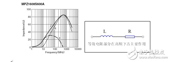
Figure 1: Impedance curve and equivalent circuit topology reflecting magnetic bead resistance, inductive reactance and total inductive reactance.
The total impedance is described by the following formula (1):
Z=(R + 2Ï€FL)
Through this curve, the magnetic beads having the largest impedance in the frequency range where the attenuation noise is desired and the signal attenuation as low as possible under low frequency and direct current are selected.
The impedance of the chip bead will be affected by the excessive DC voltage. In addition, if the operating temperature rises too high or the external magnetic field is too large, the impedance of the bead will be adversely affected.
The use of chip beads or chip inductors is mainly in application. A chip inductor is required in the resonant circuit. When it is necessary to eliminate unwanted electromagnetic interference noise, the use of chip beads is the best choice.
Tuner board EMC design
The tuner board mainly includes a tuner section and an audio processing section.
When carrying out the circuit design of the tuner board section and the PCB board layout, pay special attention to the problem of electromagnetic interference. The following points must be considered:
1. First, separate the ground of the TUNER part (ie, the simulated ground) from the ground of other parts.
2. Be sure to connect the metal casing of TUNER to the ground. More connection points can better eliminate electromagnetic interference. There is a high-frequency circuit inside the tuner TUNER, so it is necessary to do the shielding work.
3. When selecting the interface terminals (such as AV terminal, S-VIDEO terminal, etc.), try to use terminals with good conductivity and strong electromagnetic interference resistance. It is also necessary to connect the ground used for the interface terminals to the ground. Magnetic bead filtering is also added.
4. The signal line should be as short and straight as possible. If it is unavoidable, a flying line transition can be taken. Do not form a ring of signal lines. Since the ring corresponds to the number of turns of the coil, the ring wire has the strongest radiation effect.
5. Minimize large areas of dead copper. The solution is to connect them to the ground. If a large area of ​​dead copper forms an antenna, electromagnetic interference will be introduced.
6. Do not route underneath the quartz crystal and below the noise sensitive device.
Special attention should be paid to the audio processing part. In the layout of the printed circuit board, the high-speed signal line and the audio and video lines should be avoided. For example, if the clock line SCL and the data line SDA in the I2C bus are closely connected to the audio line. Since the clock line SCL and the data line SDA in the I2C bus are constantly changing, the sound is disturbed. Obviously, if you can use the TV remote control to switch TV channels, you can hear the regular "squeaky, squeaky" sound from the speakers. This may be because the above problem is neglected when printing board layout.
Machine EMC design
The assembly drawing in the whole machine (taking one of the models as an example) is shown in Figure 2:
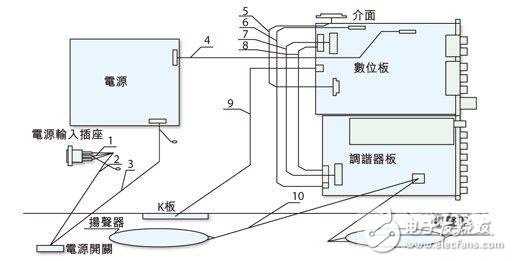
Figure 2: Assembly diagram of a complete model of the machine that reflects each EMI concern.
The connecting line labeled 5 in the above figure is the screen line of the digital board connecting screen. Since the screen line is mainly the data of the upper screen and the like. It can cause a lot of interference to the system. The best way to reduce interference is to use twisted pair and shielded wires. If it is a TTL screen, the screen line needs to be shielded or shielded outside the cable. If the LVDS screen, you need to use twisted pair cable, plus magnetic ring. To reduce the electromagnetic interference of the screen line to the entire system. With shielded twisted pair, the signal current can flow on the two inner conductors, and the noise current flows in the shield layer, thus eliminating the coupling of the common impedance, and any interference will be induced on both conductors at the same time, so that the noise is cancelled. .
A magnetic ring is also required on the connection between the power supply and the main control board (labeled 4). Mainly because the power line will cause relatively large electromagnetic interference to the main board.
A magnetic ring should also be added to the connecting line between the keypad and the motherboard (labeled 9). The main reason is that there is constant data conversion (remote control receiver) on the keypad, which causes electromagnetic interference to the system. The magnetic ring can effectively shield electromagnetic interference.
Add a magnetic ring to the audio cable (labeled 10) connected to the speaker to reduce the electromagnetic interference of the audio output to the system. If there is a cable (reference number 6, 7, 8) connection between the main board and the tuner board, you need to add a magnetic ring to the connection line. To reduce electromagnetic interference between the cables.
The magnetic ring added above can be added according to the specific situation, and can be determined by repeated experiments.
Shield use: Typically, shields are required for liquid crystal display modules, main control boards (including digital boards and tuner boards), and power sections.
The main frequency of the main chip is the main cause of electromagnetic interference. The frequency harmonics of the main frequency are most likely to generate electromagnetic interference. In the EMC experiment, the local electromagnetic interference of the frequency harmonics of the main frequency is very large. In the design, it is necessary to add certain shielding measures to the main chip. The main shielding measures are to add a metal shield to the digital board. Adding a shield is the most effective way to resist electromagnetic interference. However, because of the heat dissipation problem of the drive board and the entire system, the opening of the shield is required to dissipate heat. However, its maximum size must be less than 1/100 of the shortest wavelength of noise.
The shielding on the tuner board is mainly the shielding of the TUNER part.
The shielding of the power supply section is especially important. If the shielding of the power supply section is not good, it will cause large interference. This conduction will not pass. And because the heat generated by the power supply is very powerful, the shield must pay attention to the problem of heat dissipation.
Usually the shield has openings and seams that can cause electromagnetic leakage. Therefore, the shielding effect is not good. The solution to the electromagnetic leakage at the seam is to use an electromagnetic sealing gasket at the seam. The electromagnetic leakage of the opening in the shield is related to the size of the opening, the characteristics of the radiation source, and the distance from the source to the opening. The shielding requirements are met by designing the size of the opening and the distance from the source to the opening.
Author: Sun engineers will develop the Haier Group R & D Center
Enershare's commitment to future-ready energy solutions for smart home innovations, Enershare's Energy Storage Systems create a flexible energy maintenance system for homeowners who want to take more control of their home energy use, it is intended to be used for home battery energy storage and stores electricity for solar self-consumption, load shifting, backup power, and off-the-grid use. you can use it anytime you want-at night or during an outage.
Large Solar Battery System,Large Electric Power System,Large Solar Energy Storage System,Solar Energy System Unit,Solar Panel Inverter Lithium Battery Unit,Off-grid Hybrid Solar Battery Energy Storage System
Shenzhen Enershare Technology Co.,Ltd , https://www.enersharepower.com