Abstract: Study the FPGA implementation structure of the synchronization and despreading part of the core module of DS / FH hybrid spread spectrum receiver using code spread spectrum. The functions of various special chips are integrated on a large-scale FPGA chip, and the receiver is highly integrated and miniaturized. The serial-parallel hybrid acquisition algorithm and frequency hopping synchronization algorithm of pseudocode are all completed by hardware, which improves the acquisition speed. Experimental results prove that the scheme is correct and feasible.
In the DS / FH hybrid spread spectrum communication system, data conversion, related accumulators and code generators are required to complete operations such as down conversion and related despreading. A dedicated chip is usually used to complete these functions, resulting in an increase in system volume and inconvenience in miniaturization. Modern EDA (Electronic Design Automation) tools have broken through the limitations of early PCB layout design or circuit function simulation and pure software scope. With the goal of finally achieving a reliable hardware system, all tools for automatic system design are configured, such as Various commonly used hardware description language platforms VHDL, Verilog HDL, AHDL, etc .; equipped with a variety of compatible and mixed logic description input tools, such as hardware description language text input method (including Boolean equation description method, schematic description method , State diagram description, etc.) and schematic input method, waveform input method, etc .; also equipped with high-performance logic synthesis, optimization and simulation tools. FPGA is basically developed in logic devices such as PAL and GAL. Compared with PAL, GAL, etc., FPGA has a large scale and is more suitable for logic circuit applications such as timing and combination. It can replace dozens or even hundreds of general-purpose IC chips. FPGA has the characteristics of programmability and easy modification of the design scheme. The description of the internal hardware connection relationship of the chip can be stored in the download chip. Therefore, when the programmable gate array chip and the peripheral circuit remain stationary, you can replace the download chip. Implement new features. Soon after the FPGA chip and its development system came out, it was widely concerned and welcomed by electronic engineering designers worldwide. This article mainly discusses the implementation structure of a despreading and synchronization process of a DS / FH hybrid spread spectrum receiver based on code spreading. The core of the hybrid spread spectrum receiver is implemented by the ALTERA company's APEX20K200RC240-1 device and its development platform Quartus II— — Despreading and synchronization module. 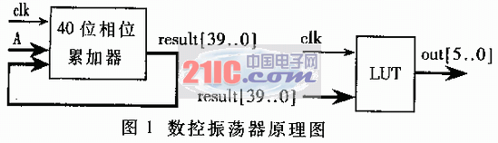
1 FPGA design of despreading module of hybrid spread spectrum receiver
The despreading module is the core of the hybrid spread spectrum receiver. This module realizes the despreading processing of the received signal, mainly including digital down-converter, digital control oscillator (NCO), code generator, related accumulator and pseudo-code phase shift circuit, etc. Usually each module uses a dedicated chip. Using FPGA to integrate these functions in a single chip greatly reduces the size of the receiver and facilitates the miniaturization and integration of the system. The FPGA implementation structure of each part of the module is introduced below.
1.1 Numerically controlled oscillator (NCO)
The numerically controlled oscillator is an important part of the despreading module, which is mainly used to provide an accurate clock signal for the code generator, so as to realize the capture and tracking of the received signal. The code generator consists of a phase accumulator and a look-up table. If an accumulator with a word length of 40 bits is used, for a certain frequency control word A, the relationship between the output frequency fout and the input frequency control word A is:
fout = fclkA / 2 40
Among them, fclk is the system clock. As long as the size of the control word A is changed, the output frequency fout can be controlled. The minimum step size Δf for Fout change is determined by the data width of the accumulator. If the data width is 40 bits, then:
Δf = fclk / 2 40
Using the above principle, the desired frequency can be obtained through accurate frequency division. The schematic diagram is shown in Figure 1. 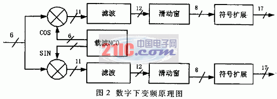
The frequency control word A in Figure 1 is written by the DSP. Considering the limitation of FPGA internal storage resources, the upper eight bits of the 40-bit phase accumulation value result [39..0] are taken as the input of the lookup table LUT (look ~ up table), which is composed of ROM and stores the samples corresponding to each phase value. When the input end of the look-up table is a certain phase phase, the corresponding sampling value is output. If the output data width is 6 bits and the output signal format is a cosine signal, the LUT output is:
out [5..0] = 31 & TImes; cos (360 & TImes; (phase + 0.5) / 256) ° + 32
If the parallel 6-bit out [5..0] of ROM is used as the output, the output signal is a digital cosine signal with 256 points sampled per cycle; if the highest bit out [5] is used as the output, the output is the frequency division of the system clock signal.
1.2 Digital down converter
The digital down-converter down-converts the intermediate frequency signal obtained by A / D sampling, removes the interruption, and obtains the baseband signal. Use local NCO to generate sine and cosine signals with the same frequency as the input IF signal, and perform complex multiplication with the input signal, and then perform low-pass filtering on the operation result to complete the down conversion of the IF signal. In quadrature sampling mode, two A / D converters provide quadrature inputs IIN and QIN, and the complex multiplier outputs IOUT and QOUT of the digital downconverter are:
Iout = IINcos (ωt) -Qinsin (ωt)
Qout = IINsin (ωt) + Qincos (ωt)
The local oscillator signal, complex multiplier, and low-pass filter are all digitally designed. The digital down converter adopts APEX20K200RC240-1 device of ALTERA company. The typical gate number of the device is 200,000, with rich logic units and RAM units, the development platform Quartus II comes with macro modules, lpm_mult (multiplier macro module), lpm_rom (ROM macro module), lpm_add_sub (adder macro module) Etc., which brings great convenience to the design. The schematic diagram of the digital down converter is shown in Figure 2. 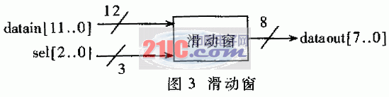
The numbers in Figure 2 indicate the data width of the corresponding module. The filter module is a second-order low-pass filter that filters out high-frequency components after mixing. In some special digital down-converter devices, STEL-2130, the order of the filter is programmable, and different orders can be set as needed to obtain different filtering effects. Considering the FPGA resource problem, the order of the filter is set to a fixed second order. The relationship between filter input x [n] and output y [n] is:
y [n] = x [n] + x [n-1]
y [n-1] = x [n-2] + x [n-3]
The low-pass filter adds two adjacent input data as output, that is, every two input data corresponds to one output data, and the input data clock tick is twice the output data clock tick. 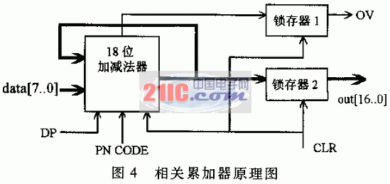
The data after low-energy filtering is processed by a sliding window, which selects and outputs the input data to dynamically adjust the size of the correlation peak. When observing the correlation peaks during the capture process, by adjusting the sliding window, the correlation peaks of different amplitudes can be obtained. Choose the control port DSP to write the control word to decide, the structure is shown in Figure 3. The logical relationship of the sliding window control is:
CASE sel [] IS
WHEN 0 => dataout [] = datain [7..0];
WHEN 1 => dataout [] = datain [8..1];
WHEN..2 => dataout [] = datain [9..2];
WHEN 3 => dataout [] = datain [10..3];
WHEN 4 => dataout [] = datain [11..4];
WHEN 5 => dataout [] = datain [12..5];
WHEN OTHERS => dataout [] = datain [12..5];
The sign extension is to keep consistent with the data width of the related accumulators behind, and the sign bit extension needs to be consistent with the sign of the highest bit of the input data. 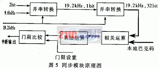
1.3 Related Accumulator
The correlation accumulator completes the correlation accumulation operation of the local pseudo code and the received signal, and the result obtained by the operation is sent to the DSP to complete the capture and tracking of the pseudo code. The length of the pseudo code is 256 bits, and half-chip sliding is adopted, and 512 accumulation operations are completed in one code period. If the serial sliding correlation acquisition method is adopted, the time required to traverse all code phases is 512 code periods, that is, the maximum time required for acquisition is 512 PN code periods. Due to the development of programmable logic devices, there are sufficient hardware resources to complete parallel operations. The serial / parallel mixed acquisition method is adopted here, and 8-channel correlation accumulators are used, each channel is divided into three groups of lead, current, and lag, each group differs by half a chip phase, and each channel differs by 64 half-chip phase . In this way, it is only necessary to slide 64 half-chip phases to traverse all pseudo-code phases, and the time required to complete the acquisition is shortened to one-eighth of the original. Data demodulation is done by another 4 groups of related accumulators. Because the phase of the synchronization pseudo code and the data pseudo code at the transmitting end are strictly aligned, in the receiving module, after the synchronization pseudo code is captured and tracked, the obtained phase information is directly used in the data demodulation correlator to correctly demodulate the data.
Synchronization pseudo-code tracking uses a lead-lag delay phase-locked loop (DPLL), and each correlator includes 3 sets of accumulators. A total of 28 groups of related accumulators are used for capture tracking and data demodulation. The structure of each group of related accumulators is exactly the same. They are divided into I and Q channels. The accumulation operations are performed separately. After 512 accumulation operations are completed, the DSP reads Fetch data. The structure of I and Q is exactly the same, and the schematic diagram of one is shown in Figure 4.
The related accumulator consists of an 18-bit adder-subtractor, latch 1 and latch 2, data [7..0] is the input data after down conversion, and PN CODE comes from the code generator. As the control terminal, the low level completes the addition operation, the high level completes the subtraction operation, the DP rising edge performs data latching, and the falling edge completes an accumulation operation. When the accumulation operation is completed, the CLR signal is cleared and the result is stored in the latch 2, the falling edge of CLKR is valid. Latch 1 outputs the OV signal as an overflow flag, and Latch 2 outputs the accumulation result out [16..0]. The highest bit of the input and output is the sign bit.
1.4 Local code generator and code phase shift circuit
The local code generator is used to generate a local PN code to perform correlation operations with the received signal. Because the transmitting end adopts coded spread spectrum modulation, there are both synchronous PN code and data PN code in the received signal. Corresponding to the received signal, the corresponding PN code should also be generated locally for synchronization and demodulation of data.
The local PN code generator is implemented by FPGA, and programmable registers and external interfaces are set. The DSP can preset the PN code length through the interface. The 1024-ary counter circuit is used to generate the input address of the ROM. The ROM is realized by the internal RAM resources of the FPGA, and uses the APEX20K200 device of ALTERA company. The internal programmable RAM capacity of the device is 106496 bits, which can meet the design requirements. The local PN code adopts the half-chip sliding mode, and the PN code inside the ROM is also stored in the half-chip mode. If the code length is 256, after half-chip storage mode is used, each group of PN codes needs to store 512 bits of data, and the corresponding ROM has 9 bits of address line driver output. The driving clock is twice that of the PN code clock. In the actual design, 8 groups of PN codes are stored in the PN code generator, but only five groups are used, one group is used for synchronization, and the other four groups are used for demodulating data. The ROM input address is generated by a 1024-ary counter. In fact, only a 512-ary counter is needed to obtain the ROM input address. Considering the scalability, a variable counter with a maximum counting capacity of 1024 is used here. Rewriting the register value by the DSP through the FPGA-FPGA interface can easily adjust the output phase of the PN code. 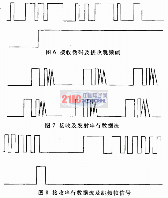
The main function of the pseudo code shift circuit is to shift the PN code generated by the code generator to obtain different phases of the pseudo code. The acquisition and tracking process uses a total of 8 groups of 24 related accumulators, each of which is divided into three groups of lead, current, and lag. The PN codes at the input of the three groups of accumulators differ by half a chip phase. Each two adjacent channels differ by 64 half chips. The code generator outputs 5 groups of PN code sequences (Group 0 to Group 4), corresponding to the synchronization pseudo code and the 4 data pseudo codes respectively. The 5 groups of pseudo codes all pass through the 512-level shift register, and the 0 groups of PN codes are used as the synchronization codes, and the 0, 1, 2 phases are taken as the input of the 3 groups of related accumulators for the leading, current, and lag of the first channel; Phase 66 is used as the input of the three groups of related accumulators in advance, current and lag of the second channel, and so on for the remaining channels. After the acquisition is completed, the synchronization PN correlation obtained by the acquisition needs to be switched to the data demodulation correlation accumulator. For example, assume that the current phase of the second group of related accumulators should be consistent with the current channel PN code phase of the second group of related accumulators. The realization of data pseudo-code phase switching is to capture the phase of the channel by the DSP memory, and then control the multiple selection switch to select the phase.
2 FPGA implementation of the synchronization module
The synchronization module is composed of a bit synchronization and frame synchronization circuit, which mainly realizes the detection and extraction of information data, and recognizes the position of the frame header of a frame of information data to realize the synchronization of frequency hopping patterns. The synchronization of the frequency hopping pattern adopts the waiting search synchronization method. At the beginning, the frequency synthesizer at the receiving end stays at a single frequency point ft ', waiting for the frequency fi of the transmitter. When the frequency of the transmitter changes to fi, the local end of the receiving end After the frequency fi 'is mixed with the transmitted frequency fi, the intermediate frequency fIF is output. After the DSP completes the despreading and demodulation operation, the obtained serial data stream is sent to the bit synchronization and frame synchronization circuits, and the feature words are extracted from the data stream to obtain a complete frame of data, thereby determining the position of the frame header, that is, the frequency At the time of conversion, since the frequency synthesizer at the receiving end and the frequency synthesizer at the transmitting end are hopped synchronously, synchronization of the frequency hopping pattern is achieved. Due to the use of coded spread spectrum modulation, every two bits of information at the sending end have a PN code period that is coded as one of four PN codes. Therefore, at each PN code period, the receiving end compares the maximum accumulation results of the four sets of data-related accumulators and then decodes them into corresponding information data. The information data is sent to the synchronization circuit to perform the correlation of mark code matching, extract valid information bits, and control the frequency hopping sequence to complete the frequency hopping synchronization. The principle of the synchronization module is shown in Figure 5.
In each PN code period, 4 sets of data demodulation related accumulators demodulate 2bit information data. 2bit information data is sent to the synchronization circuit at a rate of 9.6kHz. The synchronization circuit first converts the information data in parallel and serial, and converts the 9.6kHz and 2bit data streams into 19.2kHz and 1bit data frames. The converted data stream undergoes serial-parallel conversion to obtain a 19.2kHz and 32bit parallel data stream. According to the signal format, each frame of data is 32bit, and the position of the corresponding 13-bit Barker code in a frame of data is fixed. Therefore, the 13-bit data bits at the corresponding position in each frame of data are extracted and correlated with the local Barker code. , The result is compared with the threshold value, if the threshold setting is met, there is an interrupt output, and the external device is notified to read the corresponding data. 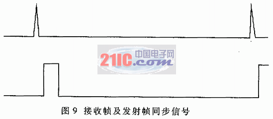
3 Experimental results
The technical specifications of the system are: information data rate 4.8kbps, bit rate 19.2kbps. The frequency hopping rate is 600hop / s, 20 frequency hopping points, the frequency hopping bandwidth is 68MHz, the 32-bit spreading code period per hop is 256, and the code rate is 4.9152MHz. Observe the experimental results with TEKTRONIX 2221A digital storage oscilloscope. Figures 6-9 are the test results of FPGA test points.
The first group of waveforms in FIG. 6 is a 256-code long local reception synchronization pseudo-code stream, and the second group is a frequency-hopping frame synchronization signal. The phase of the pseudocode corresponding to this signal is the phase of simultaneous despreading and frequency-hopping synchronization. The first group of waveforms in Figure 7 is the received data stream, the second group of waveforms is the transmitted data stream, the transmitted data frame format is 00000000011111001101010000000000, the frame synchronization code is a 13-bit Barker code 1111100110101, and the 8-bit information data is 00000000. It can be seen from Figure 7 that the data at the receiving end is the same as the transmitting end, but lags behind the transmitting end, which is caused by the transmission delay. The first group of waveforms in FIG. 8 is to receive serial data, and the second group is frequency-hopping frame synchronization signals. The falling edge of this signal corresponds to the start of a frame of data, and the frequency synthesizer is controlled to perform frequency conversion. The first group of waveforms in FIG. 9 is the transmission frequency-hopping frame signal, and the second group is the reception frame synchronization signal. The rising edge of the reception frame signal is aligned with the falling edge of the transmission frequency-hopping frame signal, and the signal width is greater than the signal at the transmitter. This is because the updata signal that controls the frequency synthesizer to perform frequency conversion needs a fixed width.
Despreading and synchronization are the key to correct data demodulation of the DS / FH hybrid spread spectrum receiver. FPGA design is used to realize the functions of multiple dedicated chips, which greatly reduces the size of the receiver and facilitates the miniaturization and integration of the system. Algorithms such as acquisition and frequency hopping synchronization are implemented in hardware to speed up acquisition and tracking. The programmability of FPGA makes the design of the circuit more flexible and makes the system have the characteristics of a "soft" receiver. Experimental results show that FPGA system design is correct and feasible.
Dog Training Transmitter,Vibration Training Collar,Remote Control Vibration Collar,Rechargeable Dog Shock Collar
Elite-tek Electronics Ltd , https://www.aetertek.ca