Abstract: A wireless digital transmission circuit composed of a wireless transmission chip TRF4900, working in the 868 MHz frequency band in Europe and the 915 MHz ISM frequency band in North America, FSK modulation, transmit power 7 dBm, power supply voltage 2.2 ~ 3.6 V, connected to the microcontroller through a serial interface Realize parameter setting and launch control. The article introduces the application circuit, the circuit connected to the microcontroller and the setting of characteristic parameters.
1 Wireless digital transmission circuit
The wireless digital transmitting circuit adopts the wireless transmitting chip TRF4900. TRF4900 is a multi-channel FSK transmitter produced by TI, monolithically integrated, low-cost, and capable of providing full functionality. The chip can meet linear (FM) or digital (FSK) transmission applications in the 868 MHz band in Europe and the 915 MHz ISM band in North America. The single-chip transmitter chip has an operating voltage of 2.2 to 3.6 V, a typical transmit power of 7 dBm, and low power consumption. The 24-bit direct digital synthesizer has an 11-bit DAC and the synthesizer has a channel space of approximately 230 Hz, allowing narrowband and wideband applications. Two fully programmable operating modes-Mode 0 and Mode 1, allow very fast switching between two pre-programmed settings (eg transmit frequency 0 or transmit frequency 1). The integrated voltage-controlled oscillator (VCO), phase-locked loop (PLL) and reference oscillator are integrated in the chip. Only a few external components are needed to form a complete transmitter circuit. The TRF4900 is connected to the TI MSP430 microcontroller via a serial interface. Each function block of the transmitter can program its function through the serial interface. TRF4900 application circuit shown in Figure 1.
Figure 1 TRF4900 application circuit
2 Connect the circuit with the microcontroller
TRF4900 is connected to TI's MSP430 microcontroller through a serial interface, as shown in Figure 2.
Pin 23 (LOCKDET) of TRF4900, PLL phase lock detection output, is effectively high. When LOCKDET = 1, the PLL is locked. Pin 11 (MODE), mode selection input, the function of the device in mode 0 and mode 1 can be programmed through the A, B, C, D words of the serial control interface. Pin 12 (), sleep control, active low. When = 0, the content of the control register is still valid and can be programmed through the serial control interface. Pin 14 (TX-DATA), digital modulation input, is FSK / FM modulation of carrier wave, high level is effective. 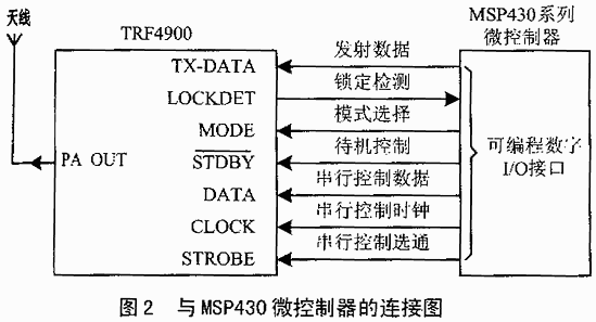
The serial control interface is a 3-wire unidirectional serial bus (CLOCK serial interface clock signal, DATA serial interface data signal, STROBE serial interface strobe signal) used to program the TRF4900. The registers inside the interface contain all user programmable variables, including DDS frequency settings, as well as all control registers. The timing of the serial interface is shown in Figure 3.
On each rising edge of the CLOCK signal, the logic value on the DATA pin is written into the 24-bit shift register. Set the STROBE terminal to high level, the programmed information is loaded into the selected latch. When the STROBE signal is high, the DATA and CLOCK lines must be low. Therefore, the signals of STROBE and CLOCK are not synchronized. The serial interface can be programmed to work in an active state or a sleep state (standby mode).
Figure 3 Serial interface timing diagram
3 TRF4900 settings
The direct digital synthesizer DDS of TRF4900 is based on the digital method to generate sine wave signal. The DDS consists of an accumulator, a sine wave look-up table, a digital-to-analog converter, and a low-pass filter. The clocks of all digital function blocks are provided by the reference oscillator. DDS uses an N-bit adder to count from 0 to 2N, and generates a digital staircase wave according to the data conversion specification in the frequency register to construct an analog sine wave. Each number in the output register of the N-bit counter is used to select the corresponding sine wave value output in the sine wave look-up table. After digital-to-analog conversion, a low-pass filter is used to suppress unwanted spurious responses. The analog output signal can be used as a reference input signal for the PLL. The PLL circuit multiplies the reference frequency by a predetermined coefficient.
The frequency fref of the reference oscillator is the sampling frequency of the DDS, and also determines the highest DDS output frequency. Together with the number of bits of the accumulator, the frequency resolution of the DDS can be calculated. The minimum frequency step size of TRF4900 can be calculated by the following formula:
Δf = N & TImes; (fref / 2 24)
The 24-bit accumulator can be programmed through two 22-bit frequency setting registers (A word determines the frequency of mode 0, B word determines the frequency of mode 1), and the two MSB bits of the register are set to 0. Therefore, the maximum bit weight of the DDS system is reduced to 1/8, as shown in Figure 4.
This bit weight is compatible with the VCO output frequency (fref / 8) × N. According to the logic level at the MODE terminal, the internal selection logic loads the DDS-0 or DDS-1 frequency into the frequency register. The output frequency fout of the VCO is determined by the DDS-x frequency setting (DSS-0 in the A word and DDS-1 in the B word). The calculation formula of the VCO output frequency fout is as follows:
fout = DDS_x × N × (fref / 2 24) = N × [(fref × DDS_x) / 2 24]
If FSK modulation is selected (MM = 0, C word, 16 bits), the 8-bit FSK frequency offset register can be used to program the frequency offset of 2-FSK modulation. The 8 bits of the frequency deviation register are in the 24-bit DDS frequency register, the LSB is set to 0, and the total FSK frequency deviation is calculated by the following formula:
Δf2-FSK = N × [(DEV × fref) / 2 22]
Therefore, the 2-FSK frequency is set by the level on TX-DATA, and the calculation formula is as follows:
fout1: TX_DATA = low = N × [(fref × DDS_x) / 2 24]
fout2: TX_DATA = High = N × [fref × (DDS_x + 4 × DEV)] / 2 24 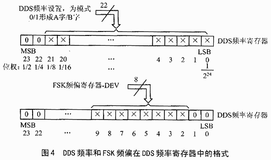
This frequency-modulated output signal is used as a reference input signal for the PLL circuit. 2-FSK modulation channel width (frequency offset) and channel spacing are software programmable. The minimum channel width and minimum channel spacing depend on the RF system frequency design, and the center frequency fcenter = (fout1 + fout2) / 2. When FSK is transmitted, the center frequency fcenter is considered to be an effective carrier frequency.
The phase-locked loop consists of a phase detector (PD), a frequency discriminator (PD), a charge pump, a VCO, an external loop filter, and a programmable prescaler (N divider) in the feedback loop. When using an external VCO, the x-VCO bit will be set to 0. The frequency divider is programmable, and the frequency division factor N can be set to 256 or 512 by the C word.
The power amplifier (PA) can be programmed by the two bits P0 and P1 in the D word to provide a variable output power level.
Figure 5 Serial control word format
The control word of TRF4900 is 24 bits. The first introduced bit is the most significant bit (MSB), which completes the programming of the TRF4900; four 24-bit words must be set, that is, the words A, B, C, and D must be set. Figure 5 shows the four control words defined. Table 1, Table 2 and Table 3 describe the function of each parameter, Table 4 is the transmission frequency in FSK mode.
Table 1 Mode 0 control register description
| Symbol | Bit position | Digits | Description | Internal settings after power on | |
| Default state | Defaults | ||||
| 0-PA | [10-9] | 2 | Power amplifier mode P1 P0 0 0 = invalid 0 1 = Attenuation 10dB, enable modulation via TX-DATA 1 0 = 20dB attenuation, enable modulation via TX-DATA 1 1 = Attenuation 0dB, enable modulation via TX-DATA | Failure | 00b |
| 0-VCO | [11] | 1 | During operation, this pin will always be enabled (1 = enabled) unless an external VCO is used | Failure | 0b |
| 0-PLL | [12] | 1 | Enable PLL, 1 = enable, 0 = disable | Failure | 0b |
Table 2 Mode 1 Control Register Description
| Symbol | Bit position | Digits | Description | Internal settings after power on | |
| Default state | Defaults | ||||
| 1-PA | [10-9] | 2 | Power amplifier mode P1 P0 0 0 = invalid 0 1 = Attenuation 10dB, enable modulation via TX-DATA 1 0 = 20dB attenuation, enable modulation via TX-DATA 1 1 = Attenuation 0dB, enable modulation via TX-DATA | Failure | 00b |
| 1-VCO | [11] | 1 | During operation, this pin will always be enabled (1 = enabled) unless an external VCO is used | Failure | 0b |
| 1-PLL | [12] | 1 | Enable PLL, 1 = enable, 0 = disable | Failure | 0b |
Table 3 Auxiliary control register description
| Symbol | word | Bit position | Number of bits | Description | Internal settings after power on | |
| Default state | Defaults | |||||
| DDS-0 | A word | [21-0] | twenty two | Mode 0DDS frequency setting | 0 | All 0 |
| DDS-1 | B word | [21-0] | twenty two | Mode 1 DDS frequency setting | 0 | All 0 |
| DEV | D word | [20-13] | 8 | FSK sub-frequency register | 0 | All 0 |
| APLL | C word | [20-18] | 3 | Acceleration factor of capture frequency A2 A1 A0 0 0 0 = 1 0 0 1 = 20 0 1 1 = 60 ┊ 1 1 1 = 140 | 0 | 000b |
| NPLL | C word | [17] | 1 | PLL frequency division 0 = 256 1 = 512 | 256 | 0b |
| MM | C word | [16] | 1 | Modulation mode selection. Setting for FSK data entry TC-DATA pin behavior. 0 = FSK / FM 1 = Not used | FSK mode | 0b |
Table 4 Transmit frequency in FSK mode (MM bit is set to 0)
| Pin end | Launch frequency | ||
| STDBY | MODE | TX-DATA | |
| 1 | 0 | 0 | fout = fref × N × (DDS_0) / 2 24 |
| 1 | 0 | 1 | fout = fref × N × (DDS_0 + 4 × DEV) / 2 24 |
| 1 | 1 | 0 | fout = fref × N × (DDS_1) / 2 24 |
| 1 | 1 | 1 | fout = fref × N × (DDS_1 + 4 × dev) / 2 24 |
Conclusion
The wireless digital transmission circuit composed of TRF4900 and MSP430 can be easily embedded in various measurement and control systems; it is used in instrument data collection system, wireless meter reading system, wireless data communication system, computer telemetry remote control system, etc.
Win3 explosive proof industrial lighting ET are build with Unique design, highly impact resistant material. Adjustable lighting height and angle, rotating and flexible focus. Fully disassembled equipment, allowing for easy transport and quick assembly.
Independent Battery can be charged individually.
4 switches for independent illumination.
Continuous lighting(all lights)>9 hours
Continuous lighting(individual light)>28 hours
Spote Light,Outside Security Lights,Defiant Motion Security Light,Motion Sensor Security Light
ZHEJIANG HUACAI OPTIC-TECHNOLOGY CO LTD , https://www.win3safety.com