Many people get confused about the reference plane of a PCB trace. A common question is: For an inner layer trace, if one side is connected to VCC and the other to GND, which one is the reference plane?

To understand this, it’s important to grasp the concept of a transmission line. In high-speed PCB design, transmission lines are essential for analyzing signal behavior and explaining various phenomena that occur in fast circuits. A basic transmission line consists of two main components: the signal path and the reference path, also known as the return path.
Signals travel through the PCB as electromagnetic waves, and the signal and reference paths together create the physical structure needed for wave propagation. From an electromagnetic perspective, these two elements form the medium through which signals move. From a current loop standpoint, the signal path carries the signal current, while the reference path carries the return current, which is why it's also called the return path.
On surface traces, the trace and the underlying plane layers form the transmission environment. The lower layer doesn’t need to be specifically a power or ground plane—it can be any conductive layer, even isolated copper, as long as it's a continuous conductor. This is what makes it function as a reference plane.
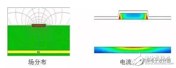
The signal path is the surface trace, and the lower plane acts as the reference path. In this case, since the reference path appears as a plane, it’s referred to as the reference plane. From a current loop perspective, it serves as the return path. The figure below shows the field and current distribution for surface traces, clearly illustrating the role of the reference plane—both as part of the electromagnetic wave transmission structure and as the return path for the signal current.
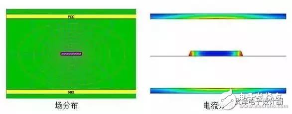
When it comes to inner layer traces, the situation becomes clearer once you understand the same logic. The trace, along with the upper and lower planes, forms the physical environment for electromagnetic wave propagation. Therefore, both the upper and lower planes act as reference paths, or reference planes. The field map below helps visualize the relationship between the physical structure and the electromagnetic field distribution.
From the current loop perspective, the return current distribution shown in the figure below further clarifies how current flows. If the distance between the trace and the two planes is roughly equal, then the return currents on both planes will be similar, making them equally important. In such cases, both planes can be considered reference planes. If you're still unsure, take a closer look at the diagram. The symmetry between the two planes should make it clear why both are valid reference planes.
The simplest way to understand a reference plane is to think of it as the physical structure that supports the transmission of electromagnetic waves.
Does the structure in question meet this condition?
Can a wide network of isolated copper areas serve the purpose?
Of course, but for a layer to be considered a reference plane, it must be flat and continuous. Otherwise, it's just a regular conductor.
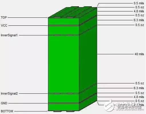
Earlier, we mentioned that when the spacing between the trace and the two planes is approximately equal (a common scenario in multilayer boards), both planes have similar influence on the signal. However, in real-world designs, one plane may be much closer to the trace than the other. For example, in a typical 6-layer board, the core thickness is often around 1 mm or more. Let’s look at a sample 6-layer stackup. Both InnerSignal1 and InnerSignal2 are inner layers, and their proximity to the surrounding planes varies significantly.
Let’s examine the return current on the VCC plane for InnerSignal2. As shown in the figure, the signal current is 10 mA, while the return current on the VCC plane is only about 1.2 mA. Most of the return current (nearly 90%) returns through the GND plane directly beneath InnerSignal2, indicating that the GND plane has a much greater impact on the signal than the VCC plane.
Now let’s consider the effect of the VCC plane on the inductance of the InnerSignal2 trace. The following figure compares the trace impedance with and without the VCC plane. Even when the VCC plane is removed, the change in impedance is minimal—less than 1 ohm, or less than 2% in percentage terms. From an engineering perspective, this means that the closest GND plane is effectively the reference plane for InnerSignal2.
Although it's reasonable to approximate the reference plane as the nearest GND plane, it's important to remember that the VCC plane isn't completely ineffective—it just has a smaller impact. Don’t overcomplicate things; understanding the relative importance of each plane is key. Avoid getting stuck on absolute answers, especially for beginners. Always keep an open mind, because overthinking can lead to confusion.
In high-speed circuit design, many issues are like this. Instead of focusing on whether something is present or not, focus on how much influence it has. This mindset helps you make better decisions when designing complex boards and ensures you’re always prepared for unexpected situations.
Universal Meter,Multi-Function Multimeter,Electronic Multimeter,Electronic Volt-Ohm-Ma Meter
YINTE TOOLS (NINGBO) CO., LTD , https://www.yinte-tools.com