Design rules and techniques for high-performance audio amplifiers
Many traditional high-power audio amplifiers now have an output power of more than 100 watts per channel, and most of them use separate circuit components. Therefore, in order to ensure the stability of the output and sound effects, engineers usually need to spend a lot of energy to match and adjust the high-definition audio amplifier.
This article takes National Semiconductor's audio driver LME49810 as an example. This component can provide a peak-to-peak output voltage swing of 200V and can drive different types of output stages. Monitors, subwoofers, audio / video receivers, commercial sound reinforcement systems, non-original audio, professional-grade mixers, distributed audio and guitar amplifiers, etc. In addition, it is also suitable for various industrial audio systems with high voltage and low distortion requirements. It can provide a more streamlined design for audio systems, help designers to develop high-performance audio systems more easily, achieve higher stability and consistency, and greatly reduce the separation and matching of separate components during system development and production.
Design tips
There are many ways to design high-quality audio systems using National Semiconductor's audio drivers. The following are design suggestions.
Input stage: The input stage design is the most critical part of the amplifier. By subtracting the signal from the feedback, the input stage will generate an error signal, and then drive this error signal to the output. The error signal is usually small enough to provide sufficient linearity for the amplifier.
LME49810 is a bipolar input amplifier, its input impedance matching is very important. Due to the bias current from the positive input port and the negative input port, the input impedance mismatch will cause the input offset voltage. The input offset voltage will be amplified according to the infinite loop gain. Of course, the input bias current of the LME49810 is very low, and for general applications, the offset voltage that appears at the output can be ignored.
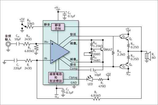
Figure 1: Schematic diagram of input stage and feedback application.
In general, there are two types of audio input designs commonly used: AC or DC coupled input. The advantage of AC-coupled input is that the input DC offset of the amplifier from the preamplifier, filter stage or codec stage is generally zero, and there is no need to add any DC servo circuit in the amplifier to prevent DC failure. The advantage of DC-coupled input is that it does not require the use of large-sized and expensive AC-coupling capacitors; low-frequency distortion caused by AC-coupling capacitors does not occur; and the noise of AC-coupled RC networks can be reduced.
Negative feedback coefficient: The negative feedback setting of the power amplifier can bring higher stability and linearity to the system. The phase shift occurs when the amplifier is operating at high frequencies, and a large negative feedback coefficient can reduce instability and oscillation at high frequencies. In split amplifier systems, high feedback coefficients will cause poor transient response or high frequency instability. However, LME49810 has a higher open-loop gain, so its dead-loop gain error and power supply ripple suppression will be smaller, which can maximize the negative feedback in the circuit, thus improving the linearity of the system. Generally, a voltage gain of 30dB to 40dB is recommended.
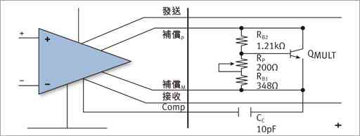
Figure 2: Output bias circuit structure.
Compensation: The amplifier's compensation is used to adjust the open-loop gain and phase performance so that the system can be stabilized when feedback is turned off. Generally speaking, the higher the stability compensation, the better. However, the greater the compensation, the lower the bandwidth and slew rate of the audio chip, and a lower slew rate will cause the system to produce softer audio characteristics. True audio characteristics. LME49810 Miller compensation is achieved by inserting a capacitor between the 'Comp' and 'BiasM' pins. The most suitable capacitor value range is 10p to 100p. In addition, the equivalent series resistance (ESR) of the compensation capacitor should be low to avoid potential zeros caused by the equivalent series resistance of the capacitor. In general, ceramic capacitors are better than electrolytic capacitors.
Mute: The MUTE pin is controlled by the amount of current flowing in. From 50uA to 100uA is the 'PLAY' mode, and below 50uA is the 'MUTE' mode. It is recommended not to let the current flowing into the MUTE pin exceed 200uA.
Output bias: LME49810 has two dedicated pins (BIASP and BIASM) for setting bias, which can provide a certain output bias current. The variable resistor Rpot can be used to adjust the bias current of the output stage. Lowering the resistance of Rpot + R b1 can increase the bias voltage. The multiplier QMULT is used to compensate the bias voltage to prevent thermal drift of the bipolar output transistor. QMULT must be connected to the same heat sink as the output transistor.
Output transistor: The most common output stage in an audio power amplifier is the emitter follower shown in Figure 3. It is often referred to as a dual-emitter follower or Darlington tube. The first follower will be the driver of the output stage.
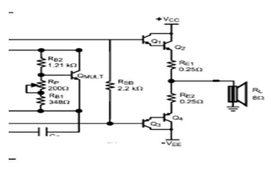
Figure 3: Output shot follower.
The linearity of the large signal of the emitter follower mainly depends on the size of the load. As the load increases (ie, the load resistance decreases), the output current will also increase. Affected by RE and β roll-off at high current density, the BJT current gain is reduced. In this case, it may reduce linearity and increase distortion at the output stage. For higher power applications, it is recommended to use a multi-level output to maintain high current and better linearity. The LME49810 audio driver has an output current of about 50mA, which can be configured as a Darlington tube or parallel transistor output as required.
Output stage transistor amplification matching: double-emitter-follower or Darlington tubes usually have a high current gain coefficient Ic = βIb. In order to improve the stability of the output stage, the current amplification of the negative terminal and the positive terminal must be matched.
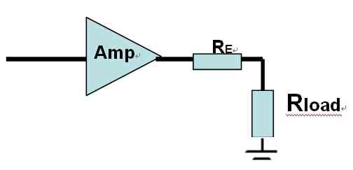
Figure 4: Application of the negative feedback resistance of the emitter.
For parallel transistor configurations, the drive capability of medium power transistors must be determined. The output current (Ic) of the medium-power transistor must be greater than the minimum drive current (Ib) of the high-power transistor to avoid overload on the medium-power transistor stage.
Output transistor voltage range: The maximum range of VCBO and VCEO voltage must be greater than the rail-to-rail range of the supply voltage. For an amplifier with a supply voltage of +/- 100V, the voltage rating of the transistor should be a little higher to ensure that it can operate normally within the specifications.
Emitter Resistor RE: In high-power audio amplifier applications, the matching, current balance, and protection of the output transistors are very important for the linearity of the power amplifier. It is recommended to use the emitter negative feedback resistor RE to improve the matching and current balance capability of the output transistor. Therefore, we recommend adding this resistor to the actual high-power audio amplifier application. However, connecting RE in series with the output transistor reduces the linearity of the amplifier. Resistor RE is the main source of distortion for crossover distortion. This distortion occurs when one end of the output transistor is turned off and the other end is turned on. Therefore, it is necessary to optimize the RE value and maintain the RE at a low level as much as possible, which can reduce the influence on the nonlinearity.
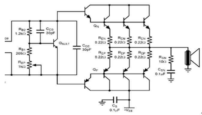
Figure 5: The output configurable structure of the audio amplifier.
The most effective way to improve crossover distortion is to reduce the resistance of RE. For REs of the same value, a parallel output can reduce the overall RE resistance value used to improve linearity. At the same time, if the RE of each stage is larger, it can bring better matching and current balance to the output transistor. In addition, RE is also related to the output power loss. For an identical RE, a larger output current will cause a larger power loss. The value of RE depends on the number of parallel output transistors and the load of the speaker. It is recommended to use 0.1 to 0.5Ω resistors with sufficient power.
Output network: The most commonly used output network for power amplifiers is 'Zobel'. All output networks have only one goal, which is to improve the stability of the system. Another function of the 'Zobel' network is to protect the output of the amplifier from the inductance in the speaker coil. The 'Zobel' network proposed here has resistors and capacitors connected in series, and the output from the amplifier is connected to ground.
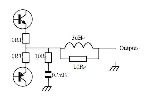
Figure 6: Output matching circuit of professional audio amplifier.
The role of the resistor in Figure 6 is to limit the current at a higher frequency to alleviate the rating requirements for the capacitor. The resistance value of the resistor ranges from 4.7Ω to 10Ω. In most cases, the value of the capacitor is selected to be 0.1μF to reduce the load effect of the output speaker at high frequencies. As the output level increases, the current captured into the 'Zobel' network will also increase. Therefore, the rated power of the components in the output network must be sufficient under any conditions, and it is recommended to be 3W to 5W. Affected by the output impedance, cable impedance, and inductance of the amplifier connected in series, the frequency response of a real speaker will exhibit unstable characteristics, which is more complicated than a simple parallel resistor and capacitor. This phenomenon may cause high-frequency instability.
A small coil inductance in series with the output of the amplifier will increase stability. This approach can isolate the amplifier from the associated capacitors without causing significant losses at the audio frequency. The inductance value is generally 1 to 7μH. Choosing the appropriate inductance value can avoid high-frequency roll-off under a certain load impedance. It is recommended to use air-core inductors to avoid magnetic saturation. In addition, it is also recommended to add a damping resistor across the output coil to reduce the Q factor, overshoot and ringing of the output LC network. Traditionally, winding damping resistors with several ohms have been used to avoid self-inductance. The lower the resistor, the less effective the overshoot and ringing. Because the size of the output current depends on the output power and load impedance. Therefore, 1W to 5W rated damping resistor should be selected.
Summary of this article
With the market development of high-end audio systems, professional-grade amplifiers require greater output power, higher linearity, and higher stability. The National Semiconductor audio driver can provide engineers with more valuable designs, allowing them to create more high-performance and highly stable audio amplifier systems.
Led Panel Light,Led Flat Panel Ceiling Light, Flat Panel Ceiling Light, 50w Led Ceiling Lights
Shenzhen Dianjiang Engineering Co. LTD , https://www.isourceled.com