Application of μPD16305 in plasma display
The performance characteristics of the row drive chip μPD16305 dedicated to plasma displays produced by NEC and its application in PDP display systems are introduced. It provides a drive signal of up to 180V for the drive circuit of the PDP scan electrode, and the display effect is satisfactory.
Keywords: plasma display, high voltage drive, μPD16305
Plasma Display Panel (PDP) is a new type of flat panel display device developed in recent years. It uses ultraviolet rays generated by gas discharge to excite phosphors to display images. It has the advantages of ultra-thin appearance, flat display, high brightness, wide viewing angle, and is not affected by the magnetic field. It is the mainstream development direction of large-screen wall-mounted TVs. However, its driving voltage is as high as 180V, so some commonly used display drivers cannot meet the high driving voltage requirements of PDP. For example, the HV53 / 5408 produced by Supertex for field emission displays (FED) can only provide a driving voltage of 90V.
In order to reduce the cost of the drive circuit and reduce the volume of the drive circuit, we used the μPD16305 high-voltage driver of NEC Company as the drive circuit of the PDP. Practice has proved that the driving circuit designed with μPD16305 as the core is simple and easy to adjust, occupies small volume and has good display effect. The performance characteristics of this chip and its specific application in the PDP drive circuit are briefly introduced below.
1 Performance characteristics
μPD16305 is a row driver dedicated to AC-PDP launched by NEC. It uses a high-voltage CMOS structure in the process. It consists of a 40-bit bidirectional shift register, a latch and a high-voltage CMOS driver block. The power supply voltage of the logic block is 5V (CMOS level input), and the drive block can achieve high voltage and high current output of 200V and 400mA. It also has the following characteristics: on-chip integrated 40-bit bidirectional shift register; low power consumption (1mW); wide operating temperature range (-40 ~ +85 ℃).
In order to make the package of the chip consistent with the standard package, μPD16305 uses a standard QFP plastic package of 80 pins. However, the 64 pins useful for the chip are led out from the three directions of the chip, and the pins are arranged counterclockwise on the chip. There are 40 high-voltage output pins, 10 power pins, 1 logic input pin and 1 logic output pin, 6 control pins, and 6 empty pins. The function description of each pin is as follows:
O1 ~ O40 (Pin 1 ~ 20, 45 ~ 64): High voltage output
VSS1 (pins 24, 41): logic block ground
VDD1 (Pin 26, 39): logic block power supply
VSS2 (pins 22, 23, 42, 43): drive block ground
VDD2 (Pin 21, 44): drive block power supply
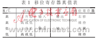
A (Pin 30): Right shift data input / output
B (Pin 35): Left shift data input / output
 (Pin 25): shift direction control terminal, when = 1, pin A is the input terminal, pin B is the output terminal, the shift register performs the right shift function;
when = 0, pin B is the input terminal, pin A is the output terminal, the shift register performs the left shift function
PC (Pin 27): Polarity reversal control terminal
CLK (Pin 31): clock input
 (Pin 32): Data clear end (active low)
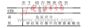
 (Pin 36): Latch enable control terminal, when = 1, execute the latch function; when When = 0, the data passes
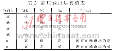
BLK (pin 37): output set control terminal, when BLK = 1, the output is in phase with the PC; when BLK = 0, the output is different from the PC or after the output
NC (Pin 28, 29, 33, 34, 38, 40): Empty pin
In order to solve the heat dissipation problem of the high-voltage chip, μPD16305 places the high-voltage output symmetrically on both ends of the chip; to facilitate the installation and debugging of the circuit, the control pins are placed on the same side of the chip.
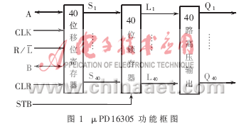
The functional structure of μPD16305 can be divided into three parts: 40-bit bidirectional shift register, 40-bit latch and high-voltage output function block. In addition to its 40-channel high-voltage output, it also has a low-voltage input and a low-voltage output. And these two input and output ports are bidirectional, when one is input, the other is output, and its output is the last bit of the shift register output. Connect this output to the input of another μPD16305, which can cascade drive more than 40 displays. For a PDP with a resolution of 852 × 480, only 12 μPD16305 are needed. Figure 1 shows the main functional blocks of μPD16305.
The truth tables of shift registers, latches, and high-voltage output blocks are shown in Tables 1, 2, and 3, respectively.
In these three parts of the circuit, the high-voltage output driving circuit is the core part of the μPD16305 chip. It provides high-voltage and high-current output for the load. The high-voltage output directly drives the display unit of the PDP screen and lights the selected pixels. Figure 2 is μPD16305 high-voltage output drive circuit diagram.
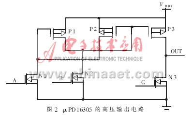
In Figure 2, the three signals A, B, and C are separated by the same signal (the signal output by the latch). They are respectively input to the three input terminals of the high-voltage output drive block, in which the A and B signals are inverted, and the A and C signals are in phase.
When A = 1, B = 0, C = 1, N1, P1, N3 are turned on, N2, P2, P3 are turned off, the output OUT = 0;
When A = 0, B = 1, C = 0, N2, P2, P3 turn on, N1, P1, N3 turn off, output OUT = VDD2.
It can be seen from the figure that this output structure is different from the ordinary complementary output structure. The advantage of this circuit structure is that it can use the digital level of the previous stage to drive the power stage circuit behind, which is not attainable for the ordinary push-pull output structure.
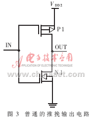 For the common CMOS complementary output structure shown in FIG. 3, it is assumed that VDD2 = 200V, GND = 0V, Vthn = 15V, and Vthp = -15V. To make Vout = GND, that is to make N tube turn on, P tube cut off, you need to satisfy ①Vgs> Vthn; ②VDD2-Vgs <-Vthp. In this way, the gate voltage Vgs should be at least equal to VDD2 + Vthp, that is, Vgs should be at least 200-15 = 185V, which requires adding a level conversion circuit to the chip to raise the CMOS digital level to a high power that can drive the power tube level. For μPD16305 with 40 outputs, it can be imagined that its volume will be huge, which is not conducive to chip integration.
Application of 2 μPD16305 in PDP drive circuit
μPD16305 is a high-voltage drive circuit with CMOS structure, which is very flexible to use. The input can be TTL level or CMOS level, and the high voltage output adjustment range can be from 0V to 200V. There is a built-in diode inside, the anode of this diode is connected to the VSS2 terminal of μPD16305, and the cathode is connected to the VDD2 terminal of μPD16305. Because there are multiple voltages on the PDP drive electrode (Y) waveform, it is impossible to complete the waveform by driving the chip PD16305 to provide a stable and constant power supply voltage. The method to solve the multi-supply voltage is to "float" the high-voltage power supply and the high-voltage ground of μPD16305, so that the power supply pin and the ground pin of the driving chip are connected to different voltages at different times, so that the output of the chip meets the corresponding requirements.
During the maintenance period, the waveforms of all Y electrodes are exactly the same. However, when scanning addressing during the addressing period, the effective time of the Y electrode of each row is different, and a variety of voltages appear. Therefore, in the maintenance period and addressing period, the different states of the MOS switch tube can be used to connect the power supply pin and the ground pin of the driving chip to different voltages at different times to obtain the desired waveform. This connection method reduces the voltage on the output stage MOS tube, which has a lot of room for application.
When driving the PDP, in the initialization phase of the maintenance period and the addressing period, the full high or low operating state of μPD16305 is used (see Table 3); while in the scanning phase of the addressing period, the shift of μPD16305 is used Working state to achieve progressive scanning.
When μPD16305 is used as a row driver, the specific connection of control signal and μPD16305 is shown in Figure 4.
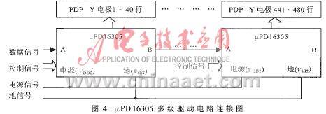
Among the control signals of μPD16305, the signal  Can be directly connected to the low voltage power supply VDD1. Because in the driving circuit, the shift function is only used in the progressive scanning stage, and the shift is performed in one direction, there is no need to add an additional signal generator and connect it to a fixed potential.
Other control signals such as A, CLK, STB, CLR, etc., can be generated with programmable logic devices based on the data measured from the PDP screen. Here we use Altera's FLEX10K10 series chips.
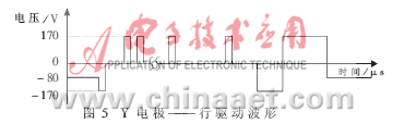
The power signal and the ground signal are provided by the level conversion circuit driving the power MOS switch tube, and the control timing of the level conversion circuit is generated by the CPLD. The resulting drive waveform is shown in Figure 5.
In practical applications, make sure that all the VDD1, VDD2, VSS1, and VSS2 pins of μPD16305 must be used, and VSS1 and VSS2 must be connected to the same potential; because pin 33 of μPD16305 is connected to the package inside the chip , So you must ensure that this pin is open and cannot be used; in order to prevent the latch-up effect of the device, you must add VDD1, then add logic signals, and finally add VDD2 in the order of power supply; in the reverse order when power is turned off To operate.
references
1 MOS INTEGRATED CIRCUIT μPD16305. NEC DATA SHEET, 1997
2 Hou Boheng. Hardware description language and digital logic circuit design. Xi'an: Xidian University Press, 1999
| About Bare Copper Wire |
Good conductivity; Strong anticorrosion; Long service life; Lowest price; Easy installation
Bare Copper Wire is used as flexible connector in electric transmission and distribution appliance(such as volt transformer, electric
stove),electronic equipment and thyristor. Underground Electrical Wire also could be used for grounding wire in electric working.
Also, it can be manufactured accordingto customer's drawings and demands.

| 1. | Professional Operation Experience |
| 2. | The Sizes All Can Be Customised |
| 3. | Sample For Your Reference Available |
| 4. | Low MOQ, Low Price |
| 5. | Safe Packing & Prompt Delivery |
| 6. | Quality Guaranted: ISO9001:2008, All Kinds of Test |
Bare Copper Wire
Bare Copper Wire,Bare Copper Wire Solid,Copper Wire Bare Copper Wire,Pure Copper Wire Bare Copper
HENAN HUAYANG ELECTRICAL TECHNOLOGY GROUP CO.,LTD , https://www.huaonwire.com