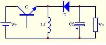
Let's dive into the discussion of the four-switch Buck-Boost converter, a popular topology in non-isolated power supply designs. While Buck, Boost, and traditional Buck-Boost circuits are well-known among engineers, the four-switch version offers some unique advantages and challenges.
In a standard Buck-Boost configuration, the output voltage is inverted relative to the input, with the formula Vo = -Vin * D / (1 - D). However, the four-switch variant changes this by maintaining the same polarity as the input, with Vo = Vin * D / (1 - D).
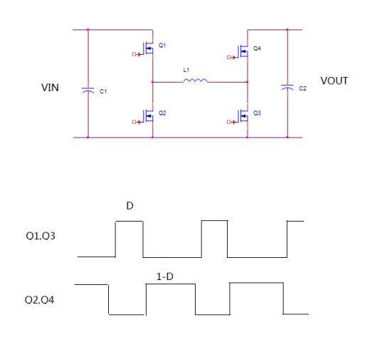
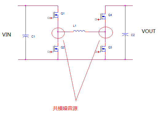
The basic structure of the four-switch Buck-Boost circuit is relatively simple, as shown below:
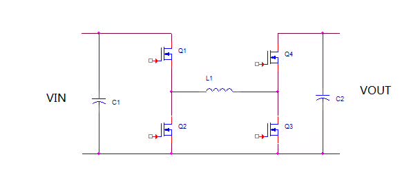
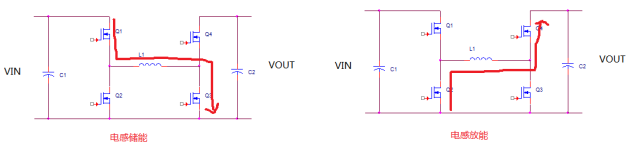
One of the key features of this topology is its control method, which is straightforward. Typically, Q1 and Q3 operate together, while Q2 and Q4 are active at different times. This alternating pattern allows for controlled switching between buck and boost modes.
If you replace Q2 and Q4 with diodes, the circuit still functions similarly, but without the benefits of synchronous rectification. This can lead to higher losses and reduced efficiency.
When operating in continuous conduction mode (CCM), the voltage transfer ratio follows the equation Vin * D = Vout * (1 - D), resulting in Vout = Vin * D / (1 - D). This is the same as the conventional Buck-Boost, except that the four-switch version provides a positive output voltage instead of a negative one.
While the traditional control method is simple and avoids mode switching, it has drawbacks. All four switches are always active, leading to higher losses and increased common-mode noise.
To address these limitations, a well-known IC company introduced a revolutionary control solution for this topology years ago. The idea was to use the four-switch Buck-Boost as a pure Buck when the input voltage is higher than the output, and as a Boost when the input is lower. This approach allows for seamless transitions between modes.
However, the real challenge lies in managing the transition when the input voltage equals the output. How do you switch smoothly from Buck to Boost, and vice versa? This became a hot topic for many companies, leading to a race for intellectual property in the field.
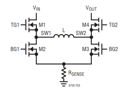
Let’s now look at the control logic used by a specific IC manufacturer. Assume the output is fixed at 12V, and the input is a battery with a full charge voltage of 16V and a discharge end voltage of 8V.
At 16V input, the converter operates in Buck mode. The driving signals for the four switches are as follows:
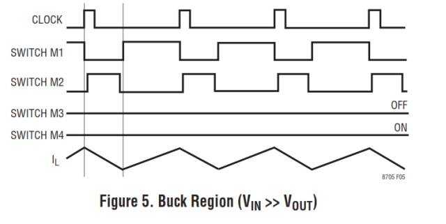
As the input voltage drops, the duty cycle of M1 increases, while that of M2 decreases. The minimum pulse width of M2 is set at 200ns, which becomes critical when the input voltage approaches the output.
For example, when the input voltage drops to 12.5V, M2’s pulse width reaches 200ns. At this point, the IC initiates a mode transition, switching M3 and M4 into operation.
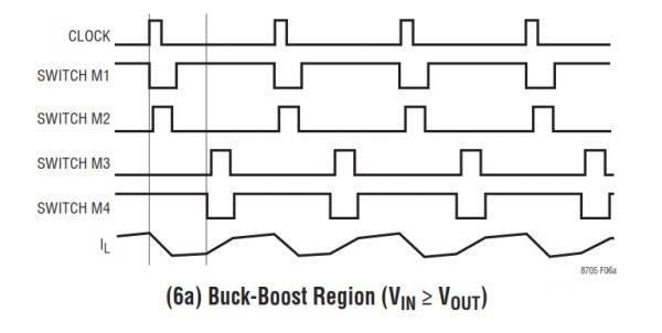
Analyzing this waveform, we observe an interesting behavior: each clock cycle consists of a Buck phase followed by a Boost phase. This allows for dynamic adjustment of the output voltage during transitions.
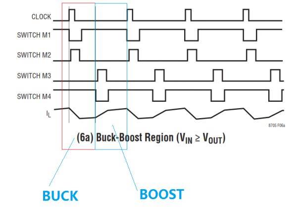
When the Boost mode is engaged, M3 operates at the minimum duty cycle, while M2 expands to compensate for the change. This results in a slight dynamic effect on the output, but the system continues to regulate effectively.
As the input continues to drop, the duty cycle of M2 keeps decreasing until it hits the minimum again. At this point, the IC triggers another mode switch, locking M2 at its minimum and allowing M3 to increase its duty cycle.
Ideally, this transition should be seamless, but due to internal timing constraints, there may be small fluctuations in the output. However, modern ICs are designed to minimize these effects.
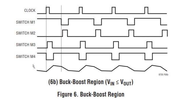
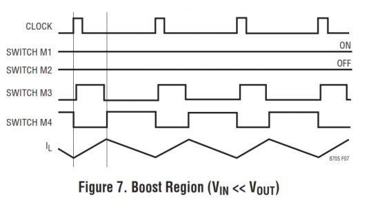
At this stage, the first half of the cycle is Boost, and the second half is Buck. As the input voltage continues to fall, the circuit eventually enters full Boost mode.
Another major player in the industry also offers a similar IC, with differences mainly in how the Buck-Boost mode is implemented. Some ICs alternate between Buck and Boost every cycle, while others divide the cycle into two parts—one for Buck and one for Boost.
Overall, both approaches achieve the same goal, though they differ slightly in implementation. These innovations have significantly improved the performance and flexibility of four-switch Buck-Boost converters in modern power systems.
Fiber Optic Accessories,Fiber Optic Cable Protection Sleeve,fiber optic cable connectors,fiber patch cables,fiber adapter
Guangzhou Jiqian Fiber Optic Cable Co.,ltd , https://www.jqopticcable.com