The choice of substrate materials is a primary consideration for the fabrication of LED chips . Which suitable substrate should be used depends on the requirements of the device and the LED device. There are currently three materials available on the market as substrates:
·Sapphire (Al2O3)
·Silicon (Si)
·SiC (SiC)[/url]
Sapphire substrate
Typically, epitaxial layers of GaN-based materials and devices are primarily grown on sapphire substrates. Sapphire substrates have many advantages: First, the production technology of sapphire substrate is mature and the device quality is good. Secondly, sapphire has good stability and can be used in high temperature growth process. Finally, sapphire has high mechanical strength and is easy to handle. And cleaning. Therefore, most processes generally use sapphire as the substrate. Figure 1 illustrates an LED chip made using a sapphire substrate.
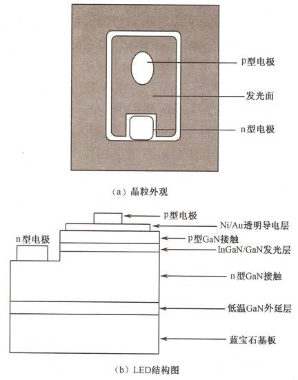
Figure 1 Sapphire as a substrate for LED chips [/ url]
There are also problems with the use of sapphire as a substrate, such as lattice mismatch and thermal stress mismatch, which can create a large number of defects in the epitaxial layer, while at the same time causing difficulties in subsequent device processing. Sapphire is an insulator with a resistivity of more than 1011 Ω·cm at room temperature. In this case, a device with a vertical structure cannot be fabricated; usually, n-type and p-type electrodes are formed only on the upper surface of the epitaxial layer (as shown in Fig. 1). The fabrication of two electrodes on the upper surface results in a reduction in the effective light-emitting area and increases the lithography and etching processes in device fabrication, resulting in reduced material utilization and increased cost. Due to the difficulty in doping P-type GaN, a method of preparing a metal transparent electrode on p-type GaN is generally used to diffuse current to achieve uniform illumination. However, the metal transparent electrode generally absorbs about 30% to 40% of the light, and the GaN-based material has stable chemical properties and high mechanical strength, and is not easily etched, so that a good device is needed in the etching process. This will increase production costs.
The hardness of sapphire is very high, and its hardness is second only to diamond in natural materials, but it needs to be thinned and cut (from 400nm to about 100nm) during the fabrication of LED devices. Adding equipment to complete the thinning and cutting process adds another large investment.
The thermal conductivity of sapphire is not very good (about 25W/(m·K) at 100 °C). Therefore, when using LED devices, a large amount of heat is conducted; especially for large-area devices with large area, thermal conductivity is a very important consideration. In order to overcome the above difficulties, many people have tried to grow GaN optoelectronic devices directly on a silicon substrate to improve thermal conductivity and electrical conductivity.
Silicon substrate
At present, some LED chips use a silicon substrate. The chip electrodes of the silicon substrate can adopt two kinds of contact modes, namely, L-contact (vertical-contact) and V-contact (Vertical-contact), which are hereinafter referred to as L-type electrode and V-type electrode. Through these two contact methods, the current inside the LED chip can be either lateral or longitudinal. Since the current can flow longitudinally, the light-emitting area of ​​the LED is increased, thereby improving the light-emitting efficiency of the LED. Because silicon is a good conductor of heat, the thermal conductivity of the device can be significantly improved, thereby extending the life of the device.
Silicon carbide substrate
The LED chip electrode of a silicon carbide substrate (CREE Corporation of the United States specifically uses a SiC material as a substrate) is an L-type electrode, and current flows in a longitudinal direction. Devices fabricated using such substrates have very good electrical and thermal conductivity properties, which facilitates the fabrication of large power devices with large areas. An LED chip using a silicon carbide substrate is shown in FIG.
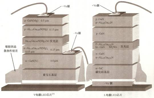
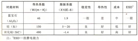
The thermal conductivity of the silicon carbide substrate (the thermal conductivity of silicon carbide is 490 W/(m·K)) is more than 10 times higher than that of the sapphire substrate. Sapphire itself is a poor conductor of heat, and the bottom of the device needs to use silver glue to form a crystal. The silver paste has poor heat transfer performance. The chip electrode using the silicon carbide substrate is L-shaped, and the two electrodes are distributed on the surface and the bottom of the device, and the generated heat can be directly led out through the electrode; at the same time, the substrate does not require a current diffusion layer, so the light is not subjected to current. The material of the diffusion layer is absorbed, which in turn increases the light extraction efficiency. However, compared with sapphire substrates, silicon carbide is expensive to manufacture, and commercialization requires lowering the corresponding cost.
Performance comparison of three substrates
The previous content describes the three kinds of substrate materials commonly used in the production of LED chips. A comparison of the overall performance of these three substrate materials can be found in Table 1.
In addition to the above three commonly used substrate materials, materials such as GaAS, AlN, and ZnO can also be used as the substrate, and are usually selected according to the design requirements.
Evaluation of substrate materials
1. The structure of the substrate and the epitaxial film are matched: the crystal structure of the epitaxial material and the substrate material are the same or similar, the lattice constant mismatch is small, the crystallization property is good, and the defect density is low;
2. The thermal expansion coefficient of the substrate and the epitaxial film is matched: the matching of the thermal expansion coefficient is very important. The difference between the thermal expansion coefficient of the epitaxial film and the substrate material may not only reduce the quality of the epitaxial film, but also cause heat due to heat during device operation. Damage to the device;
3. The chemical stability of the substrate and the epitaxial film is matched: the substrate material has good chemical stability, is not easily decomposed and corroded in the temperature and atmosphere of epitaxial growth, and the quality of the epitaxial film cannot be lowered due to chemical reaction with the epitaxial film;
4. The difficulty of material preparation and the cost: In view of the needs of industrial development, the preparation of substrate materials is simple and the cost is not high. The substrate size is generally not less than 2 inches.
There are currently many substrate materials for GaN-based LEDs, but there are currently only two types of substrates that can be used for commercialization, namely sapphire and silicon carbide substrates. Other substrates such as GaN, Si, and ZnO are still in the research and development stage, and there is still a long way to go from industrialization.
Gallium nitride:
The most ideal substrate for GaN growth is GaN single crystal material, which can greatly improve the crystal quality of the epitaxial film, reduce the dislocation density, improve the working life of the device, improve the luminous efficiency, and improve the working current density of the device. However, it is very difficult to prepare a GaN bulk single crystal, and there has been no effective method so far.
Zinc oxide:
ZnO is a candidate substrate for GaN epitaxy because of the striking similarities between the two. The crystal structure of the two is the same, the lattice recognition degree is very small, and the forbidden band width is close (the band gap is small and the contact barrier is small). However, the Achilles heel of ZnO as a GaN epitaxial substrate is easily decomposed and corroded in the temperature and atmosphere of GaN epitaxial growth. At present, ZnO semiconductor materials can not be used to manufacture optoelectronic devices or high-temperature electronic devices, mainly because the material quality is not up to the device level and the P-type doping problem has not been solved. The equipment suitable for the growth of ZnO-based semiconductor materials has not been successfully developed.
sapphire:
The most common substrate for GaN growth is Al2O3. The advantages are good chemical stability, no absorption of visible light, moderate price, and relatively mature manufacturing technology. Although the thermal conductivity is poor, there is no obvious shortage of exposure in the small current operation of the device, but the problem is very prominent in the high current operation of the power device.
Silicon carbide:
The application of SiC as a substrate material is second only to sapphire, and there is currently no third substrate for the commercial production of GaN LED. The SiC substrate has good chemical stability, good electrical conductivity, good thermal conductivity, and no absorption of visible light, but the shortage is also prominent. If the price is too high, the crystal quality is difficult to achieve as good as Al2O3 and Si, and the mechanical processing performance is poor. In addition, the SiC substrate absorbs ultraviolet light below 380 nm, which is not suitable for the development of ultraviolet LEDs below 380 nm. Due to the beneficial electrical and thermal conductivity of the SiC substrate, the heat dissipation problem of the power GaN LED device can be better solved, so it plays an important role in the field of semiconductor lighting technology.
Compared to sapphire, the lattice matching of SiC and GaN epitaxial films is improved. In addition, SiC has blue light-emitting characteristics and is a low-resistance material that can be fabricated.
- Programmable Module for ControlLogix or CompactLogix
- Industrial Wireless Solutions
- Modernization
- Oil & Gas
- Plant Energy Management
- Secure. Remote. Access.
- Water & Wastewater
-
- Modbus Master/Slave Communication Module MVI56-MCMThe MVI56 Modbus Master/Slave Communication Module allows Rockwell Automation ControlLogix processors to interface easily with other Modbus protocol compatible devices. Compatible devices include not only Modicon PLCs (which all support the Modbus protocol) but also a wide assortment of end devices. The module acts as an input/output module between the Modbus network and the Rockwell Automation backplane. The data transfer from the processor is asynchronous from the actions on the Modbus network. A 5000-word register space in the module exchanges .
-
Features and Benefits
The inRAx Modbus Master/Slave Communications module is designed to allow ControlLogix processors to
interface easily with Modbus protocol-compatible
devices and hosts.
The MVI56-MCM module acts as an input/output module
between the Modbus network and the Rockwell
Automation backplane. The data transfer from the
ControlLogix processor is asynchronous from the actions
on the Modbus network. A 5000-word register space in
the module exchanges data between the processor and
the Modbus network.
Many host SCADA packages support the Modbus
protocol, while devices commonly supporting the
protocol include several PLCs, as well as many other
third party devices in the marketplace. (For a partial list
of devices that speak Modbus, please visit the ProSoft
Tested section of the ProSoft Technology web site).
AB Prosoft Communicate Modules
AB Prosoft Communicate Modules,Communications Interface Module,Slave Communication Module,SLC Backplane Compatible Module
Xiamen The Anaswers Trade Co,.LTD , http://www.answersplc.com