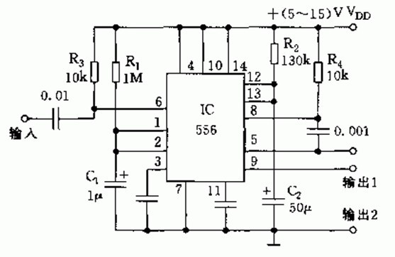
As shown in the figure, the sequence timer has a 555 as the core and constitutes a two-stage timer. Normally, the circuit is in a forced reset state due to the access of R3 and R4. When the negative trigger pulse comes, the one-shot delay circuit composed of 1/2 556 and R2, C1 triggers the timing td1=1.1R1C1, and after a delay of about one second, the second-stage stable circuit is started, and td2=1.1 R2C2, delay of about 7 seconds.
How are ceramic PCBs made?
With the emerging demand for durable, reliable miniature, high-density, high-power, and precision electronic devices, there has been a range of improvements in the design and development of these electronic devices. Therefore, engineers have conducted research in various fields of electronics, especially in the field of semiconductor electronics and printed circuit boards (PCB), integrating more electronic products into an Originality Electronics IC package. Therefore, we know the emergence of LSI and VLSI technologies, which integrate thousands of electronic circuits or gates in a single integrated circuit (originality electronics IC) package. With the passage of time, this technology has been greatly developed, and now it is necessary to improve the PCB on which these semiconductor ICs will be mounted. Therefore, designers proposed blind via hole (blind via hole PCB), buried via (buried PCB), via pad technology solutions, and introduced many other technologies to achieve high-density interconnect HDI PCB. As the density increases, power consumption also increases, thereby generating more heat. Therefore, ordinary FR-4-based substrate PCBs cannot withstand such high temperatures, and the thermal characteristics of FR-4 are not up to standard, so researchers have found a solution in the form of "ceramic substrate printed board".

1- extraordinary thermal conductivity
2- Good mechanical strength
3- High-density interconnection (HDI) is easy to implement on ceramic PCB
4- Compatibility of CTE with conductive layer, wiring and components.
5- Chemical resistance
6-Provide better high frequency performance
7-The coefficient of thermal expansion (CTE) value is low
8- can be packed in a waterproof sealed package
9- Reduce the system cost in general, especially the front-intensive packaging
10- No need for surface treatment like OSP or HASL
11-The traces can be printed with silver and protected with glass. If corrosion is a problem due to environmental conditions, gold plating can be used to protect the exposed silver pad
12-The thermal conductivity of some ceramic materials is

High temperature co-fired ceramic (HTCC) PCB:
The main components of HTCC ceramic substrates are alumina, plasticizers, binders, lubricants and solvents. The mixture will form a raw ceramic, which is then calendered and curtain coated. Tungsten or molybdenum can be used as the metal for circuit printing. Next, it was exposed to a high temperature of 1700 O C and baked in hydrogen for 32 to 48 hours. Then it is laminated and cut. This is suitable for small-sized ceramic plates, and is not suitable for large-sized ceramic plates due to inappropriate shrinkage tolerances and poor warpage
Low temperature co-fired ceramic (LTCC) PCB:
This is a combination of glass crystals and glass composite materials. In addition, other ingredients are added, such as adhesives and non-glass ingredients. Then, high-conductivity gold paste is used to create circuit traces, and then processed/baked in an oxidizing gas furnace at a high temperature of 900 O C.

Here, two alternating thick films are applied on the ceramic substrate. One is gold thick film and the other is dielectric thick film. However, because gold is expensive, copper thick film is implemented, which is a recognized technology for ceramic PCBs. The stack is then moved into a filled baking furnace (to avoid oxidation of copper), in which it is processed at a temperature of 1,000 °C in nitrogen. The dielectric paste is produced by nitrogen.
Application of ceramic PCB:
1-High-current high-brightness LED lights and spotlights.
2-Automotive electronic equipment, such as power controllers, optical systems, power converters and power conditioners
3-Industrial power equipment, such as servo drives, robots, etc.
4- Microprocessor, graphics card and IC array
5-semiconductor device
6-Audio power amplifier based on high power transistor
7-Solar battery related circuits, inverters, chargers, etc.
8- DC-DC regulator and power management circuit, etc.
Ceramic Printed Circuit Boards,Flame Resistant Pcbs,Fr-4 Pcb Laminate,Fr4 Pcb Boards
HAODA ELECTRONIC CO.,LIMITED , https://www.pcbhdi.com