The jammer introduced in this paper can generate three kinds of interference signals: random interference, point frequency interference and frequency sweep interference. The point frequency interference and frequency sweep interference are based on the control of the DDS chip AD9852 by the single-chip microcomputer. The control of the whole system is flexible and efficient. The test results show that the system can accurately generate the required interference signals and meet the needs of anti-interference performance testing. Although the interference signal generated by this design is in the 406 MHz band, such a circuit structure can also be used in other frequency bands (circuits such as VCO and PLL need to be modified), such as mobile phone communication frequency bands, so the circuit structure is also useful for other frequency bands. .
As the use of electronic devices becomes more and more common, the interference problem between electronic devices is becoming more and more prominent, especially the interference problem of communication devices, which makes circuit engineers have to consider the anti-interference of devices in the design process of electronic products. Problem, and it is necessary to test the anti-interference ability of the communication device. The RF signal jammer introduced in this paper can be used to test the anti-interference ability of communication equipment, and can generate the following three types of interference:
1) Random interference. Producing a random frequency interference signal within the target frequency range, annihilating the target frequency, also reduces the signal-to-noise ratio and forms a suppression of normal communication.
2) Point frequency interference. In the case where the target frequency is known, the target frequency is output to the interference signal, and the suppression effect on the target communication is generated.
3) Sweep interference. When the frequency sweep is performed within the target frequency range, when the collision probability of the interference signal frequency and the communication frequency reaches a certain value, the signal-to-noise ratio of the communication is affected, resulting in an increase in the bit error rate and effective interference.
The design of the RF signal jammer is based on DDS technology and phase-locked loop (PLL) technology. It can be controlled by a single-chip microcomputer to generate an interference frequency with extremely high resolution. The control is convenient and flexible.
1 hardware circuit design
The block diagram of the RF signal jammer is shown in Figure 1. When the microwave switch is turned on 406.0~406.1 MHZVCO, the random interference noise is output; when the microwave switch is turned on, the point frequency interference or the sweep interference noise is output.
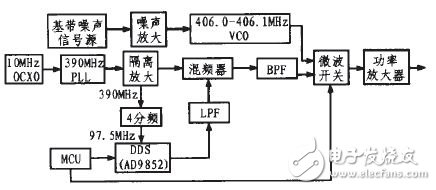
Figure 1 hardware system block diagram
1.1 Random interference
The random voltage noise of the baseband noise signal source is applied to the voltage control terminal of the VCO to generate a noise FM signal. 406.0~406.1 The frequency of the MHZVCO output signal is expressed as:
Ωvco=ωo+Kvco(Vo+Anu(t)) (1)
Where: ωo is the VCO output frequency when the control voltage is zero, Kvco is the VCO voltage control gain, Vo is the DC control voltage, An is the noise amplification circuit gain, and u(t) is the baseband noise signal.
When the microwave switch strobes the random noise output, the output signal is
Vo(t)=KSKAUvcoCOS(ωo+Kvco(Vo+Anu(t)) (2)
Where: KS is the microwave switching gain, KA is the amplifier gain, and Uvco is the VCO output signal amplitude. The output of the jammer is FM noise, the noise amplitude is KSKAUvco, and the center frequency of the noise is ωo+Kvco (Vo, the range of the noise spectrum depends on the amplitude of Anu(t).
1.2 point frequency interference and sweep interference
The point frequency interference and the sweep frequency interference are realized by the single-chip microcomputer controlled DDS special chip AD9852. The AD9852 has the advantages of low power consumption, high number of phase accumulators, and high frequency sine wave.
DDS output frequency:
F0=KF&TImes;fc/2N (3)
Among them, KF is the frequency control word, fc is the frequency of the external reference clock, and IV is the DDS phase accumulator bit number. The frequency control word of the AD9852 is 48 bits, which is N=48.
The output frequency resolution is determined by the following formula:
Δf=fc/2N (4)
According to Nyquist's theorem, the DDS external reference clock frequency is at least twice the output frequency (f0/2), but in engineering applications, the reference frequency is generally set to more than 5 times the highest output frequency. In this design, the reference frequency is 97.5MHz, and the value is substituted into equation (4). The frequency resolution of the DDS output signal is 3.5 &TImes; 10-7Hz.
The AD9852 has a built-in 12-bit DAC, and its output analog signal spectrum has fc, fc±f0 and other frequency components in addition to f0 (fc-f0 has the lowest frequency), and an LPF is designed to filter it. Here, Figure 2 is used. The seventh-order Butterworth low-pass filter shown, using the ADS simulation results for the filter, is shown in Figure 3. The attenuation at 81 MHz is -80.683 dB.
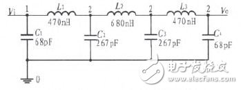
Figure 2 seventh-order Butterwoth low-pass filter
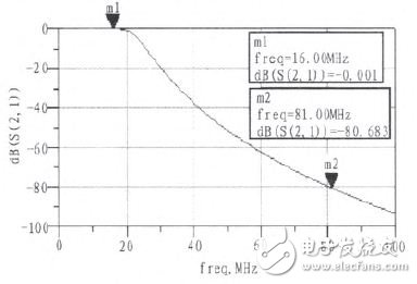
Figure 3 filter simulation results
2 software design
The AD9852 is controlled by the SPI port. The normal MCS51 MCU does not have the SPI 13. The P1 13 analog SPI port is required, and the IOUD CLK and FSK signals are provided.
The AD9852 offers five modes of operation: Single tone, FSK, Rambed FSK, Chirp, BPSK. Single tone mode outputs a single frequency, Ramped FSK mode and Chip mode can generate a sweep signal. This design uses Rammed FSK mode, and the output frequency waveform is shown in Figure 4.
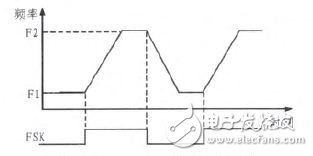
Figure 4 Ramped FSK mode output waveform
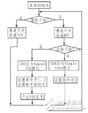
Figure 5 software main program flow chart
The main program flow chart of the MCU software is shown in Figure 5. The single-chip microcomputer selects the random interference mode or the point frequency interference through the microwave switch, sweeps the interference mode, and controls the output mode of the DDS by writing a control word to the DDS. Transform the equation (3) to get the frequency control word:
KF=f0 &TImes; 2N/fc (5)
For example, when the output frequency is 16.0 MHz, KF = 46 190 765 408928 = (2A02A02A02A0) 16.
3 test results
The three interference modes of the jammer are tested separately, and the obtained results are shown in Fig. 6(a)~(c), wherein Fig. 6(b) is the frequency scan track recorded using the maximum hold function of the spectrum analyzer. The test results meet the requirements.
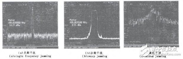
Figure 6 test results
We make OBD connector with terminal by ourselves, soldering type and crimping type are both available. Also 12V and 24V type. OBD1, OB2, J1939, J1708, J1962, etc. Also molded by different type, straight type or right-angle type. The OBD connector cables used for Audi, Honda, Toyota, BWM, etc. We have wide range of materials source , also we can support customers to make a customized one to replace the original ones.
Vehicle Diagnostic Cables,Diagnostic OBD Cable,Heavy Vehicle Diagnostic Cables,OBD2 Splitter Y Cables,OBD2 Diagnostic Adapters,OBD Heavy Vehicle Cables
ETOP WIREHARNESS LIMITED , https://www.etopwireharness.com