1 Introduction
With the continuous development of communication technology, people have higher and higher requirements for the communication rate and communication quality of information systems. In this context, ultra-wideband technology (UWB) has become a research hotspot in the field of communication. In February 2002, the US Federal Commission authorized a frequency band between 3.1 GHz and 10.6 GHz for UWB communication. As a result, research on UWB bandpass filters, which are an important part of the communication system, has also made great progress. The literature proposes a class of broadband filters based on high-loss materials with flat broadband characteristics but large insertion loss. The structure of the resonant ring and the open stub are used to implement an ultra-wideband filter, but the return loss is only 10 dB. The band pass characteristic is achieved by a combination of high-pass and low-pass filters. Parallel shorting branches are used to control the out-of-band characteristics. Multimode bandpass filters have been extensively studied for low loss and easy to process structures. In recent years, with the development of new materials and new structures, EBG structures have been introduced into the research of ultra-wideband bandpass filters.
In this paper, a class of planar ultra-wideband filters using microstrip three-wire coupling structures and parallel short-circuit stubs are proposed. The broadband transmission characteristics are realized by the coupled transmission line, and the short-circuit branch has good out-of-band rejection. The filter is simple in design, compact in structure and has good in-band and out-of-band characteristics. The insertion loss is less than 1.5dB, the return loss is higher than 15dB, and the in-band delay is less than 0.3ns. It meets the communication requirements and can be widely used in microwave ultra-wideband communication.
2, theoretical analysis
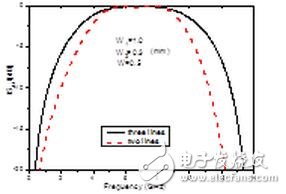
This type of ultra-wideband bandpass filter consists of two parts. Parallel coupled lines and parallel shorted branches. We know that the λg/4 coupled transmission line can achieve bandpass characteristics. The two transmission zeros are located at f0 and 2f0, respectively. To achieve greater bandwidth, we use three-wire coupling instead of two-wire coupling to increase coupling strength. As shown in Figure 1, the 3-dB bandwidth is increased from 95% to 105%. Figure 2 shows the 3-dB bandwidth as a function of the coupled linewidth (W1, W2) and bandgap width (S).
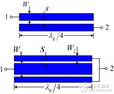
(a) Schematic
(b) Transmission characteristics S21 change diagram
Figure 1, two-wire and three-wire coupling structure

(a)
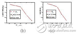
Figure 2. 3-dB bandwidth with (a) bandgap width (b) coupled linewidth (c) coupled linewidth variation
In order to obtain good out-of-band characteristics, we introduce two parallel short-circuit branches, which are located on both sides of the coupling line. Figure 3 shows the transmission characteristics of the parallel shorted stubs. We have found that as the length increases, the band gap moves toward the low frequency; as the width increases, the band gap moves slightly toward the high frequency. Thus, we can influence the bandwidth of the filter by changing the length and width of the shorting branch.
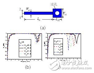
Figure 3. Schematic diagram of the parallel short-circuit branch (a). Transmission characteristics vary with (b) line width, (c) length variation
3, the design and implementation of the filter
When designing the filter, we first select the appropriate odd-mode impedance by changing the width and slot width of the coupled transmission line; then select the appropriate length and width of the short-circuited branch to ensure that the bandgap is around 12 GHz. We use the electromagnetic simulation software Microwave office to carry out the principle circuit analysis and the electromagnetic simulation software CST for 3D simulation. It was processed using a Teflon circuit board with a dielectric constant of 2.65 and a height of 1.0 mm.
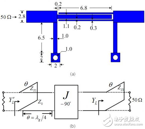
Figure 4. Schematic diagram of the designed UWB filter (a) (b) Equivalent circuit
Figure 4(a) shows the structural dimensions of the designed UWB bandpass filter. The corresponding circuit equivalent diagram is shown in Figure 4(b). The coupled transmission line acts like an admittance converter.
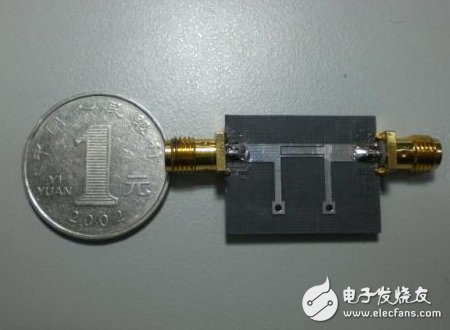
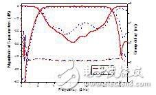
Figure 5. Comparison of the results of the (B) photo of the designed UWB filter (a)
Fig. 5(a) is a physical photograph of the designed UWB bandpass filter, and the corresponding measurement results are shown in Fig. 5(b). It can be seen that the test results are in good agreement with the simulation results, covering the entire communication range of 3.1 to 10.6 GHz. In-band insertion loss is less than 1.5dB, return loss is higher than 15dB, in-band group delay is less than 0.3ns, and out-of-band characteristics are better than 15dB.
4 Conclusion
In this paper, a class of ultra-wideband bandpass filters using a three-wire coupling structure and parallel short-circuit stubs are proposed. This type of filter uses a coupled transmission line to achieve broadband characteristics, and short-circuit branches are used to achieve good out-of-band rejection. Because of its simple design, compact size, small size, easy processing, and good in-band and out-of-band characteristics, this type of filter is suitable for wide-bandwidth communication.
Magnetic Buzzer,Buzzer Magnet,Magnetic Buzzer Transducer,Magnetic Audio Transducer Buzzer
NINGBO SANCO ELECTRONICS CO., LTD. , https://www.sancobuzzer.com