The consumer handheld device market is jumping ahead. The processing capacity of portable products is increasing, and the number of applications supported is increasing; the speed of product replacement is accelerating, new products must meet the time-to-market requirements in order to obtain the largest market opportunity; the shortening of the product life cycle requires shortening the development cycle, while emphasizing Reusability and reprogrammability. There is also an interesting trend in the emerging handheld market, where each device in a series is shipping less and less, but there are more and more customization functions between the series, which effectively increases the total shipment of the product. the amount. In this way, the key challenge becomes how to develop a system that is widely multiplexed and customizable.
This article refers to the address: http://
In response to these challenges, more and more designers are beginning to use FPGAs for handheld product development. FPGAs are becoming more powerful and richer, and the number of gates, areas, and frequencies are increasing. The development and turnaround time of FPGAs is much shorter than custom ASICs, and the additional advantages of reprogramming make FPGAs an attractive solution in the field of handheld embedded systems. In ASIC- or FPGA-based designs, designers must carefully consider certain performance criteria, and their challenges are primarily in terms of area, speed, and power consumption.
As with ASICs, vendors also need to address area and speed challenges in FPGA design. As the number of gates continues to increase, FPGAs require larger areas and sizes to accommodate more applications, and design tools require better algorithms to make more efficient use of area. Evolving FPGA technology also presents designers with a new set of challenges, and power utilization is one of them, which is an urgent problem for designing FPGA-based embedded systems for handheld or portable devices.
FPGA in embedded systems
A typical embedded system consists of a processor, memory, standard interfaces including USB, SPI, I2C, and peripherals such as liquid crystal displays and audio outputs. The core of the device is still the processor and processor interface, which are connected to the various peripherals via onboard wiring. System performance is primarily dependent on processor performance, and processors typically have a very standard architecture and are therefore not easily customizable.
Sometimes the processor may be busy processing information from low-speed peripherals, although processor utilization may reach 100% in this case, but not in microprocessor-centric transactions, but at very low performance. Level. Regardless of its core frequency, the microprocessor must wait for data from the low speed clock. This also leads to higher power consumption because the processor utilization is 100%. The result is shorter battery life and the need for larger heat sinks or fans for cooling, ultimately affecting overall system reliability.
As a result, FPGAs have begun to play an important role in this because they can offload many peripheral interaction tasks from the processor. As shown in Figure 1, an embedded distribution system of uncompressed audio and video data streams implemented using a standard Gigabit TCP/IP network. It has a dedicated DSP processor that interfaces with Xilinx FPGAs via a standard bus interface, which in turn is connected to various low-speed peripherals.
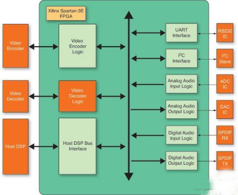
Figure 1: FPGA Architecture for Audio/Video Distribution Systems
As a start-up development kit, this FPGA connects a 12-bit PCM audio input and a 12-bit PCM audio output through an I2S interface; it also connects to a video encoder and decoder and communicates with I2C slaves and RS232 devices; connected to the FPGA There is very little general purpose I/O. The standard bus connected to the processor operates at a high speed of 66 MHz, while the audio peripheral operates at a low speed of 1.182 MHz; the UART and I2C serial interfaces operate at 56.6 kHz and 100 kHz, respectively. Since data transmission occurs in multiple clock domains, only the processor can configure the data stream.
In this case, the processor no longer interacts with the low-speed peripherals, and the FPGA reads the data from the low-speed PCM ADC audio device and stores the data in the FPGA's internal cache. The processor can periodically read data from this cache, or an interrupt is sent by the FPGA to the processor when there is enough data in the cache. In this way, the processor has more time to perform the necessary processor-centric work and enters sleep mode when idle.
Power consumption problem
In battery-operated embedded systems, energy savings are the most important consideration. Power consumption can be divided into three broad categories: startup power, static power, and dynamic power. Designers have no control over startup power, and startup power plays an important role in determining power supply selection. Most of the maximum current values ​​refer to the values ​​reached at this stage. However, static power and dynamic power are two different areas. With reasonable planning and the following correct guidelines, embedded designers using FPGAs can make significant improvements in power optimization.
Static power consumption refers to the power consumption generated when current flows through the device when the system is not operating. It is generally caused by the device bias current and leakage current. Static power consumption also depends on the operating voltage. Lowering the operating voltage reduces static power consumption, but this strategy is not always in the hands of designers. What designers can do is to define a reasonable architecture in which the resources needed to be used are the least, while using resource sharing as much as possible and using the FPGA modules in the most efficient manner.
Another technique to reduce static power is to estimate power consumption early in the design cycle, change the topology or use different IP blocks. For example, Xilinx's xPower Estimator tool is very useful at this point, and it knows early whether the design meets the power budget. The power estimation in the early stages may not be completely accurate, but it is really helpful as a guiding tool.
Dynamic power consumption is caused by some behavior of the FPGA gate (such as signal switches), which will generate current flow and capacitance when the two gates are temporarily turned on. The speed of the signal switch determines the amount of power consumed. Another factor that affects dynamic power consumption is the inherent capacitance formed in the internal structure of the circuit. Dynamic power consumption is a function of the clock frequency, the number of gates being switched, and the rate at which these gates are switched. Capacitive loads on the fan-out and trace lines increase dynamic power consumption, and the power dissipation value is proportional to the product of capacitance, voltage, and frequency squared.
Designers have the most control over this power consumption, and they can use many techniques to achieve the greatest improvement in dynamic power consumption. Reducing the signal switching frequency can cause the power consumption to decrease exponentially. As shown in Figure 1, control logic, parity, or frame overrun errors for the UART occur in the slower clock domain. Even if the number of gates is not reduced, power consumption will decrease. Designers can also reduce dynamic power consumption by reducing the overall operating frequency (if applicable). For example, after completing the feasibility and performance analysis, the designer decided that the above design can work not only at 133MHz but also at 66MHz. The DSP supports both rates, and reducing the voltage also helps to reduce power consumption.
Another technique is to reduce the number of effective gates in the operating mode. Sometimes some of the logic is turned on and configured at boot time, but it doesn't actually require anything to do. For example, the analog audio capture unit is active and the device is not performing any digital SPDIF audio capture. In this case, the general digital SPDIF audio capture circuit will still perform data sampling, two-phase decoding, etc., thus wasting power unnecessarily. If the entire digital SPDIF audio capture circuit is disabled so that no signal switching occurs in the circuit, the dynamic power consumption will be significantly reduced.
Designers can disable the clocks sent to this part of the circuit to achieve this. A simple approach is to "AND" the clock signal with the enable signal, as shown in Figure 2. If the enable signal is low, the output of the AND gate will remain low. If the enable signal is high, the AND gate will output a clock signal.
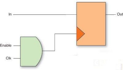
Figure 2: A simple clock gating mechanism
Other methods can also be used. If possible and the topology supports it, you can reduce the number of signal lines by multiplexing the address and data lines. In our example, the output to the video encoder is 16-bit data, which we can multiplex into 8 bits and then send them out on both edges (rising and falling edges) of the clock. This also saves dynamic power. In addition, the choice of a serial interface instead of a parallel interface also reduces power consumption. It is also useful to use LVTTL or LVCMOS I/O with a lower capacitive load.
Embedded processor
Embedding the processor into the FPGA is another strategy that handheld device designers can take, which can bring many benefits. First, the above challenges of custom processors are reduced. Second, the interaction between the peripheral and the processor takes place inside the FPGA, thus reducing the number of I/Os. Since I/O consumes a considerable amount of power, this can also achieve a certain degree of energy savings. Xilinx's Virtex-5 version supports the PowerPC 440 processor, hard processor and MicroBlaze soft processor, all of which can be used by designers to create high-end or low-end applications.
With the invention of 90m and 65nm semiconductor technology, the size of the door is shrinking, resulting in more and more outstanding static power problems. This is a very challenging phenomenon in today's increasingly sensitive to power consumption indicators. As power consumption issues have gained the attention of many FPGA vendors, many exciting new technologies have emerged in this area. Low-power design will determine how well a system's integration capabilities are, and there is an urgent need in the industry to standardize power-conscious design techniques.
iPhone XS Max Tempered Glass compatible with iPhone XS MAX 2018. 2.5D or 3D arc edge is smooth to the touch and do not scratch your fingers. Explosion-proof 9H hardness scratch-resistant Screen Protector can effectively protect your iPhone XS Max from high impact drops, scratches, scrapes, bumps, puncture. Nano technology processing for Oleophobic coating which prevent fingerprints on surface of screen. High definition and high transparency to allow a natural viewing experience.
Description of iPhone XS Max Tempered Glass
Size: 6.5 inch
For iPhone XS Max
Material: Corning, Schott or AGC
Radian: 2.5D / 3D
Technology: Clear / Anti glare / Anti blue light / Privacy / Printing
MOQ: 1K pieces
Packaging: Standard export package or Customized
Payment: T/T, Paypel, Others
Delivery: In Shenzhen CHINA, 2.5D: 7-10 working days / 3D: 15-20 working days after your payment
FAQ:
Q1: Are you a trading company or manufacturer?
---A: We are distributor located in Shenzhen, China.
Q2: Is the sample free?
---A: Yes, the free sample will be sent for your evaluation!
Q3: What is the production lead time?
---A: 2.5D: 7-10 working days / 3D: 15-20 working days after your payment.
Q4: Do you inspect all your goods before delivery?
---A: Yes, we have 100% inspect before delivery.
Welcome to make inquiry!
IPhone XS Max Tempered Glass
IPhone XS Max Tempered Glass,2.5D IPhone XS Max Tempered Glass,9H IPhone XS Max Tempered Glass,Tempered Glass For IPhone XS Max
Shenzhen Kantou IM Technology Co., Ltd. , https://www.kantou-im.com