Switching regulators are a popular choice for many power conversion circuits due to their size, output flexibility, and efficiency advantages. Depending on the operating conditions, the conversion efficiency of this type of power supply can now reach 98%. However, despite these advantages, such power supplies must compromise on other parameters, the most difficult of which is noise.
However, what is the “noise†of a switching regulator? To better understand this term, let us start with the fact that switched mode power supplies produce broadband harmonic energy. This kind of energy that people don't want comes in two forms, radiation and conduction. In the industry, they are often called "noise." However, this name is not accurate enough because the output "noise" of the switching regulator is not noise at all, but the naturally remaining high-frequency component directly related to the switching of the regulator. The correct name for this phenomenon is electromagnetic radiation, or the more common name is EMI. Moreover, indeed, EMI has both forms of radiation and conduction.
Since in many circuit applications, to achieve optimal performance, a noise-free, well-regulated power supply is important, it is important to reduce the noise that is inherent in this conversion process. An obvious way to reduce noise is to use a linear regulator. However, while linear regulators provide very low noise rails, their conversion efficiency is poor at high step-down ratios, which can cause thermal problems in the design of large output current applications.
Accordingly, switching regulators typically have higher conversion efficiencies than linear regulators, so the thermal design of the switching regulator is simpler when the final application requires large output currents. One can understand that component selection and board layout play a very important role in determining the success or failure of almost all power supplies. These aspects determine the EMI and thermal performance at runtime. For the layman, the switching power supply layout may seem magical, but in fact, in the early stages of design, this is often a fundamental aspect of neglect. Since it is always necessary to meet the EMI requirements at runtime, then it is good for power supply stability, which is usually good for reducing EMI emissions. In addition, determining a good layout from the start does not add any cost to the design, and in fact, it can save costs by eliminating the need for EMI filters, mechanical shielding, EMI test time, and numerous circuit board modifications. .
In addition, when multiple switch-mode DC/DC regulators are used in a single design to generate multiple rails, if these regulators are connected in parallel to share current and provide greater output power, it is possible to aggravate noise. Potential interference problems. If all regulators operate (switched) at a similar frequency, the combined energy generated by multiple regulators in the circuit may be concentrated near a single frequency. The presence of this energy can be problematic, especially if the remaining ICs on the printed circuit board (PCB) and other system boards are close together and susceptible to this radiant energy. This is especially problematic in industrial and automotive systems because such systems are densely packed and very close to electrical noise sources such as mechanically switched inductive loads, PWM driven power outputs, microprocessor clocks and touches. Point switch. In addition, if switching at different frequencies, the intermodulation components may alias into the sensitive frequency band.
Switching regulator radiationIn industrial, medical, and automotive environments, low heat dissipation and high efficiency are important for applications, so switching regulators are often used instead of linear regulators. In addition, switching regulators are typically the first active component on the input power bus and therefore have a large impact on the EMI performance of the entire product design.
Conducted radiation depends on the wires and traces that are connected to the product. Since the noise is limited to a particular terminal or connector in the design, as already mentioned above, it is often possible to ensure that the conducted emission requirements are met relatively early in the development process through a good layout or filter design.
Radiated EMI is another matter entirely. Everything that carries current on the board radiates an electromagnetic field. Each trace on the board is an antenna, and each copper plane is a resonator. In addition to a pure sine wave or DC voltage, any signal produces noise across the signal spectrum. Even after careful design, the power supply designer never really knows how serious radiated EMI is before the system is tested. The radiated EMI test will not be formally completed until the design is basically completed.
Filters are often used to reduce EMI and reduce the intensity of interference at a certain frequency or frequency range. By adding metal shielding and magnetic shielding, it is possible to attenuate that portion of the energy radiated through the space. By adding ferrite beads and other filters, you can reduce the amount of energy (conducting radiation) that depends on the PCB trace. EMI cannot be completely eliminated, but can be attenuated to acceptable levels for other communications, signal processing, and digital components. In addition, several regulators have implemented standards to ensure compliance with industrial and automotive system requirements.
New input filter assemblies with surface mount technology perform better than through-hole assemblies. However, this improvement is less than the ever-increasing demands of today's high-frequency switching regulators. Very short minimum on and off times are required at higher operating frequencies, resulting in higher harmonic components due to faster switching transitions, thus increasing radiated noise. However, to achieve higher conversion efficiency, such a high switching speed is required. Switched-capacitor charge pumps do not have this problem because they operate at much lower switching frequencies and, most importantly, can tolerate slower switching without reducing efficiency.
A skilled PCB designer will design a small thermal loop and place the shield ground plane as close as possible to the active layer. However, to store sufficient energy in the decoupling component, there are certain requirements for device pinout, package structure, thermal design, and package size that determine the minimum thermal loop size. To complicate matters, in typical flat printed circuit boards, magnetic or transformer-type couplings above 30 MHz between traces will attenuate all filtering effects because the higher the harmonic frequency, the more effective the unwanted magnetic coupling.
Another solution to EMI problemsWhat has been tried to really solve the EMI problem is to use a shielding box for the entire circuit. Even then, the shielding cannot completely prevent the coupling of sensitive circuits in the box. Of course, this increases cost, increases board space requirements, makes heat management and testing more difficult, and adds additional assembly costs. Another method that is often used is to reduce the switching speed. This approach has the undesirable effect of reducing efficiency, extending the minimum on/off time and associated dead time, thus reducing the potential current control loop speed.
A few years ago, Linear Technology introduced the LT8614 Silent Switcher® regulator, which provides the desired shielding box without the need for a shielded box, while eliminating many of these shortcomings. However, in some noise applications, power supply designers do not like to use inductor-based regulators due to the associated EMI emissions. At the same time, linear regulators (ie LDOs) may also be excluded due to the relatively low conversion efficiency and the need for a heat sink. As a result, the designers turned to another common method called a charge pump.
Charge pumps have been around for decades, providing DC/DC voltage conversion and charging and discharging two or more capacitors with a switching network. The basic charge pump switch network switches between the charging and discharging states of the capacitor. As shown in Figure 1, C1 is a “floating capacitor†that carries the charge and C2 is the “storage capacitor†that holds the charge and filters the output voltage. Adding "floating capacitors" and switch arrays offers a number of benefits.
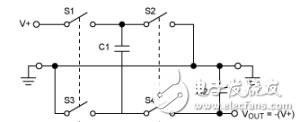
Figure 1: Block diagram of a simplified charge pump for a voltage inverter
When switches S1 and S3 are turned "on" or "off", switches S2 and S4 are turned "off" or "on" and the input power supply charges C1. In the next cycle, S1 and S3 are disconnected, S2 and S4 are turned on, and charge is transferred to C2, producing VOUT = -(V+).
However, until recently, charge pumps have provided limited input and output voltage ranges, which limited their use in industrial and automotive applications where inputs of up to 40V or 60V are common. However, with Linear Technology's introduction of a high-pressure charge pump, this situation has now changed.
High pressure charge pumpThe LTC3245 is a buck-boost regulator that rejects the traditionally used inductor and uses a switched capacitor charge pump. The input voltage range is 2.7V to 38V and can be used without a feedback divider to generate one of the two fixed output voltages, 3.3V or 5V, or 2.5V to 5.5 via a feedback divider. Any output voltage in the range of V. The maximum output current is 250mA. The LTC3245 is capable of regulating the output voltage above or below the input voltage to meet the automotive cold-start requirements. See the full schematic of Figure 2.
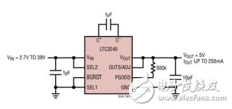
Figure 2: LTC3245 schematic with fixed 5V output from 2.7V to 38V input
This charge pump delivers 80% efficiency with a 5V/100mA output from a 12V supply, which is almost twice the linear regulator, making it possible to avoid the high space and cost requirements of an LDO with a heat sink. The charge pump consumes almost three times less power than the LDO at full load. See Figure 3 for the LTC3245 efficiency and power curve.
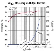
Figure 3: LTC3245 Efficiency/Power Curve for 12V Input to 5V Output
EFFICIENCY: Efficiency
5VOUT Efficiency vs Output Current: 5VOUT, efficiency varies with output current
The LTC3245 also features excellent radiated and conducted EMI performance, as shown in Figures 4a and 4b. These measurements were taken in a miniature container that meets CISPR22 and CISPR25 requirements. As can be seen, after proper decoupling, the LTC3245 does not pose any problems in meeting government regulatory requirements for radiated and conducted EMI.
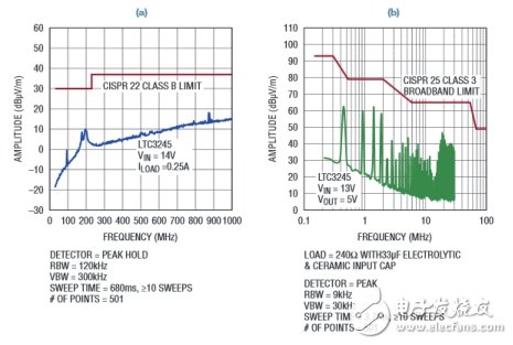
Figure 4: Radiation (a) and conduction (b) EMI of the LTC3245
AMPLITUDE: Amplitude
CISPR22 CLASS B LIMIT: CISPR22 CLASS B Limit
FREQUENCY: Frequency
DETECTOR = PEAK HOLD: Detector = Peak Hold
SWEEP TIME: scan time
10 SWEEPS: 10 scans
# OF POINTS: Points
CISPR25 CLASS 3 BROADBAND LIMIT: CISPR25 CLASS 3 Broadband Limit
LOAD = 240Ω WITH 33μF ELECTROLYTIC & CERAMIC INPUT CAP:
Load = 240Ω and 33μF electrolyte and ceramic input capacitor
DETECTOR = PEAK: detector = peak
In many industrial, medical, and automotive applications, electronic products such as op amps, drivers, and sensors often require bipolar power supplies. However, it is rare to use a bipolar power supply at the point of load. Due to this need and the lack of an easy-to-use solution, Linear Technology developed the LTC3260.
The LTC3260 is a negative output charge pump DC/DC converter with two low noise LDO regulator followers that can generate positive and negative supplies from a single 4.5V to 32V input supply, as shown in the full schematic of Figure 5. The device switches between high-efficiency Burst Mode® operation and low-noise constant current frequency mode, allowing designers to make the best trade-offs for their applications.
The LTC3260 can supply up to 100mA at the charge pump output VOUT with an inverting input voltage. This VOUT also acts as the input voltage to the negative LDO regulator LDO-. The charge pump frequency can be adjusted from 50kHz to 500kHz with a single resistor. Each LDO of the LTC3260 can support loads up to 50mA. Moreover, each LDO has a 300mV dropout voltage at 50mA, and an output resistor divider network can be used to set the output voltage. When both regulators are disabled, the shutdown quiescent current is only 2μA.
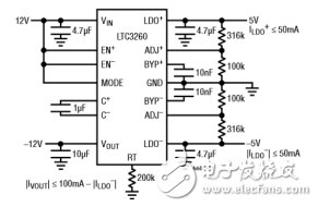
Figure 5: 12V input supply to ±5V output
in conclusionIt is well known that at the beginning of design, EMI issues for industrial, medical, and automotive environments require careful attention to ensure that EMI testing is passed once the system is complete. Until now, there is no sure way to succeed, ensuring that EMI testing is easily passed at the end by choosing the right power IC, except for systems with very low power.
Linear Technology recently introduced low EMI regulators and DC/DC converters, including an extensive line of linear regulators and LT86xx Silent Switcher step-down converters. Now, our growing range of high pressure charge pumps offers a third option. These products offer much higher efficiency and much lower power consumption than linear regulators, and do not need to deal with compensation, layout, magnetic field, and EMI issues associated with switching regulators.
Ethernet cable wiring serviced offered for CAT5 and CAT6 by UTP, STP FTP. And DB and RJ series in different pins, all related tool is available. We have developed a tradition of high-tech engineering, prototyping, and quality custom cable manufacturing at very competitive pricing. Also with professional flow chart (wire cutting-stripping-copper twisting-crimping-crimping 100% inspection-soldering-molding-asssembling-braiding-testing-FQC100% -OQC) , which can help us support customers with stable quality.Such as cat 5 wiring cable,cat 5 cable.
Ethernet Cable Wiring,Cat 5 Wiring Cable,Custom Wire Assembly,RJ45 Cable,Cat 5 Cable,Cat 5 Wiring Cable
ETOP WIREHARNESS LIMITED , https://www.etopwireharness.com