First, Pkg and PCB system
As people's demand for data processing and computing becomes higher and higher, the core of electronic products - the process size of chips is getting smaller and smaller, and the frequency of work is getting higher and higher. At present, the core frequency of the processor has reached Ghz, and the digital signal is more Short rise and fall times also bring higher harmonic components, and the digital system is a high frequency, high bandwidth system. For an assembled PCB, both the PCB itself and the package (Package, Pkg), the resonant frequency of the geometry also falls within this range. Improper power supply system (PDS) design will cause structural resonance, resulting in deterioration of power quality and system failure.
In addition, due to the increase in component density, in order to reduce system power consumption, the system generally adopts a low voltage and low swing design, and the low voltage signal is more susceptible to noise interference. These noise sources are very wide, such as coupling, crosstalk, electromagnetic radiation (EMI), etc., but the biggest impact comes from the noise of the power supply, especially the Simultaneous Switching Noise (SSN).
In general, the entire PDS system includes an electromagnetic field system formed by a power source and a ground plane in addition to the circuit system. The figure below is a schematic diagram of a power transmission system.
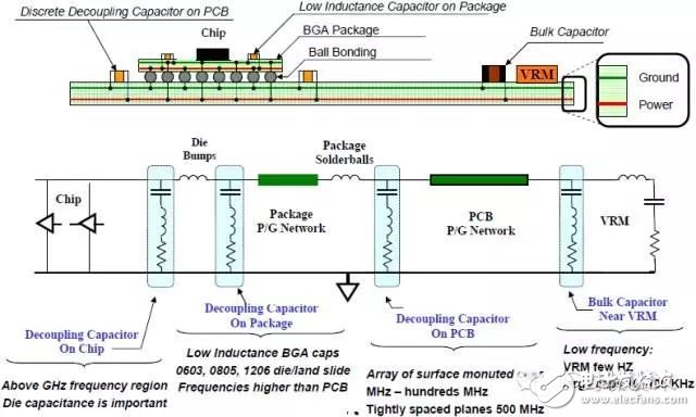
Figure 1 Schematic diagram of a typical power transmission system
Second, Pkg and PCB system measurement
Generally, when discussing ground bounce noise (GBN), usually only consider PCB, and measure its S parameter |S21| to indicate the basis of GBN size. Port1 represents the location of the SSN excitation source, which is the location of the active IC on the PCB, while the smaller |S21| represents a better PDS design and a smaller GBN. However, the general noise is generated from the IC, through the Pkg power system, and then through the connection between the substrate Via and the solder ball on the package, to the power system of the PCB (Figure 1). Therefore, we can't just consider PCB or Pkg, we must combine the two to correctly describe the behavior of GBN in high-speed digital systems.
To this end, we designed a PDS structure (Figure 2) to represent the Pkg power system installed on the PCB.
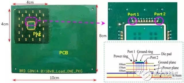
Figure 2 Schematic diagram of the structure and cross section of the BGA package mounted on the PCB
The S parameters of this structure were measured using a network analyzer (HP8510C) in combination with a probe station (Microtechprobe staTIon) from 50 Mhz to 5 Ghz. For measurement, two 450um-pitch GS probes were used, connected to the Powerring and Ground ring of the Pkg signal layer. This measurement structure is shown in Figure 3.
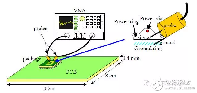
Figure 3 Schematic diagram of structural measurement of the BGA package mounted on the PCB
The results of the Pkg+PCB structure measurement S parameters are shown in Figure 4. At the same time, we also made a single Pkg and PCB measurement results, through comparison to understand the difference between the entire PDS system and a single Pkg and PCB.
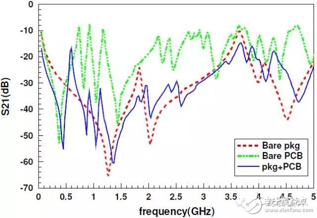
Figure 4 Measurement results of the BGA package mounted on the PCB
From the measurement results in Figure 4, we can see that the GBN behavior of the three structures is very different. First consider the S-parameter with only a single Pkg. The behavior before 1.3Ghz is like a capacitor. After 1.5Ghz, there is a resonance mode. Considering a single PCB, there is a resonance mode after 0.5Ghz, like 0.73Ghz ( TM01), 0.92Ghz (TM10), 1.17Ghz (TM11), whose GBN behavior is worse than a single Pkg. Finally, considering Pkg combined with PCB, it can be seen that before 1.5Ghz, there are three more resonance points than a single Pkg. These noise resonances come from the PCB and are coupled to the Pkg power supply through solder balls, Via, etc., which will make Pkg The IC is more affected by noise, which is quite different from considering only a single Pkg or PCB.
Third, the effect of decoupling capacitors on power supply noise
The traditional method of suppressing power plane noise is to use that coupling capacitor. There have been many studies on the use of decoupling capacitors, but the size, position, and number of capacitors are basically based on empirical rules.
Ideal location for decoupling capacitors
In order to study the effect of the decoupling capacitor position PDS, we use the above Pkg+PCB structure, add decoupling capacitors on Pkg and PCB, or both add decoupling capacitors, and measure the ideal of decoupling capacitors by measuring |S21| Place the position.
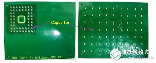
Figure 5 Decoupling capacitors mounted on Pkg and PCB
As shown in Figure 5, we placed the position of the capacitor in three cases. One is to add 52 to Pkg, the other is to add 63 to the PCB, and the third is to place 52 and 63 at the same time on Pkg and PCB. The capacitance value is 100nF, and the ESR and ESL are 0.04 ohm and 0.63 nH, respectively. The measurement results are shown in Figure 6.
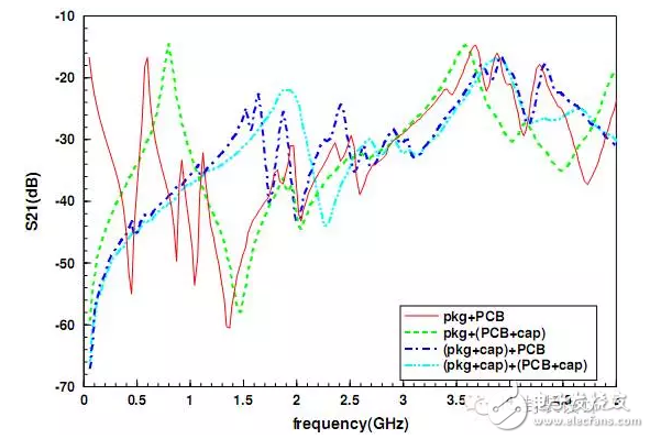
Figure 6 |S21|Comparative diagram with decoupling capacitors at different positions
First, divide the low frequency into 5Ghz into three stages. First, start the low frequency to about 500Mhz. No matter the decoupling capacitor is added to the Pkg or PCB, the structure impedance can be greatly reduced and the GBN interference can be reduced compared with no capacitor. Second, for 0.5Ghz ~ 2Ghz, adding decoupling capacitors on Pkg and PCB at the same time, the noise suppression effect is similar. However, if you only add a capacitor to the PCB, you can see that there is one more resonance point near 800Mhz, which is worse than when no capacitor is added. Therefore, we only pay special attention when adding capacitors on the PCB. The power supply noise may be more serious after the capacitor is added. Third, from 2Ghz to 5Ghz, the three capacitors are less effective than the capacitors, because this phase exceeds the resonant frequency of the capacitor itself. Due to the influence of the capacitor ESL, the coupling capacitor increases with the frequency. Gradually loses its effect and loses its inhibitory effect on higher frequency noise.
Decoupling capacitor ESR effect
On the Pkg combined with the PCB structure, place 12 decoupling capacitors and change the ESR of the decoupling capacitor. The simulation results are shown in Figure 7. It can be found that when the ESR value is getting larger, the pole will be leveled and the zero point will be filled, making S21 a relatively flat curve.
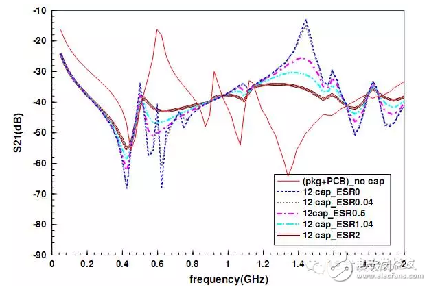
Figure 7 Effect of ESR of decoupling capacitor on |S21|
Decoupling capacitor ESL effect
On the Pkg combined with the PCB structure, place 12 decoupling capacitors and change the ESL of the decoupling capacitor. The simulation results are shown in Figure 8. From the figure, we find that the larger the ESL, the larger the amplitude of the resonance point, and the tendency to move to the low frequency, the lower the ability to suppress noise.
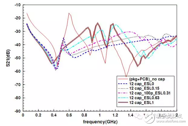
Figure 8 Effect of ESL of decoupling capacitor on |S21|
The effect of the number of decoupling capacitors
From the previous results, it is known that the capacitor is better placed on the package, so the discussion on the number of capacitors is mainly on the Pkg. In the structure of the aforementioned Pkg+PCB, the placement of the capacitor on the Pkg is shown in Fig. 9, and the simulation result is shown in Fig. 10.
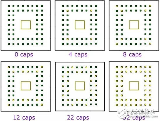
Figure 9 Location of the capacitor on the package
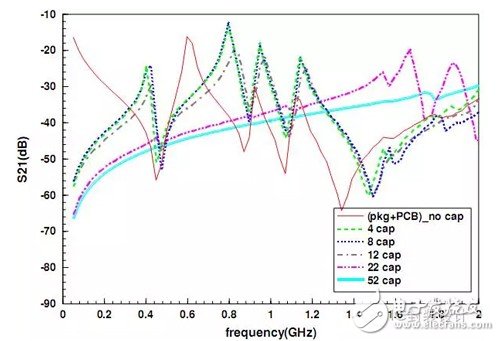
Figure 10 Effect of the number of capacitors on |S21|
It can be seen from the measurement results that when 4 and 8 are added, at 0 to 200 Mhz, |S21| can be effectively depressed, but a new resonance point is generated near 400 Mhz, and the subsequent resonance point is moved to a high frequency. When 12 to 52 pieces are added, the low frequency |S21| is also depressed, and the resonance point near 400 Mhz is greatly reduced, the high frequency resonance point is shifted to the high frequency, and the amplitude is greatly reduced.
As the number of capacitors increases, the suppression of noise is better, from 4 to 8 300Mhz to 1.2Ghz (52), so increasing the number of capacitors helps to improve the noise suppression capability of the power supply.
Decoupling capacitance value
On the combined structure of Pkg and PCB, capacitors with different capacitance values ​​are placed, and the simulation results are shown in Fig. 11.
For the comparison between adding 100nF and 100pF, the 100n large capacitance has better suppression effect between 0 and 300Mhz; 500~800Mhz, 100p small capacitance has better effect; and adding 100n capacitance will resonate with the whole system structure at 400Mz When using 100n+100p, 200~600Mhz, it is worse than simply using 100n and 100p, and there is no single value in lower frequency or higher frequency; when using 100n+1n+100p three kinds of capacitance, it produces more Resonance point, especially in the electronic system, if the noise generated by the circuit is just at the resonance frequency point, the noise is amplified, affecting or radiating the signal.
Therefore, the choice of the capacitance value should be determined according to the frequency band to be suppressed. After the frequency band is determined, the capacitance is selected according to the resonance point of the capacitor. The lower the capacitance, the better the ESL and ESR.
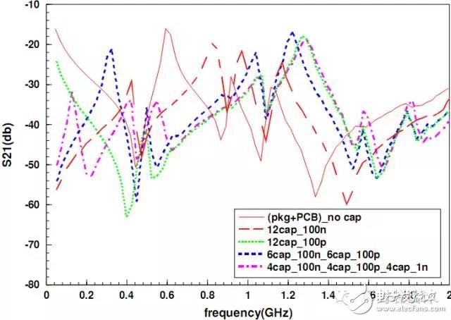
Figure 11 Simulation results of mixing different capacitance capacitors
Effect of slab thickness
First, the distance between the fixed PCB power supply and the ground plane is 0.7 mm, and the thickness of the Pkg power supply layer is changed to 1.6 mm, 0.8 mm, 0.4 mm, and 0.15 mm, respectively. The result is shown in Figure 12; when the thickness of the Pkg power layer is more and more High, the first zero point moves to the low frequency; from the previous conclusion, the noise before 2Ghz comes from the PCB. From the result, the noise from the PCB coupling is also increased, and after 2Ghz, it is mainly affected by the package, you can see |S21| It also becomes larger with thickness, so the thickness of the Pkg power plane has a large influence on the S parameter.
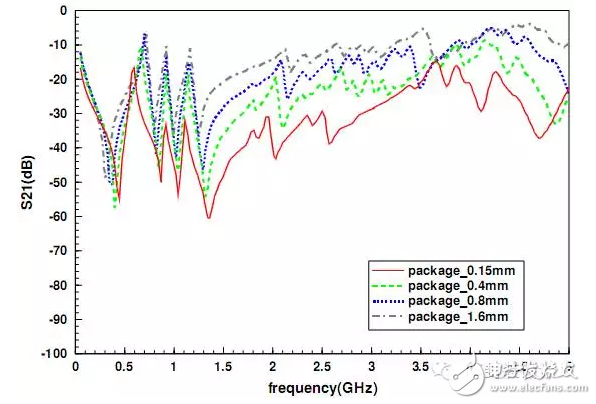
Figure 12 Effect of different Pkg power layer thickness on |S21|
Next, we fixed the Pkg thickness to 0.15mm, and changed the PCB thickness to 0.15mm, 0.4mm, 0.8mm, and 1.6mm respectively. The effect of PCB thickness on the S parameter is shown in Figure 13. The PCB power layer thickness can be seen as a whole. The trend has little effect, only the low frequency part has little difference, the thickness increases by the first zero point and the small high frequency moves, and the high frequency part only slightly differs.
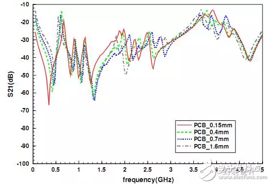
Figure 13 Effect of different PCB power layer thickness on |S21|
Effect of capacitance placement distance
We know that the position of the decoupling capacitor is as close as possible to the noise source, because it can reduce the inductance between the capacitor and the noise source, allowing the capacitor to absorb the glitch faster, reduce the noise, and stabilize the voltage. Also reducing the thickness of the power plane can reduce the parasitic inductance of the power plane and can also do the same. In the simulation, we change the distance between the capacitor and the test point, which are 1.7cm and 0.2cm respectively. The thickness of Pkg and PCB power layer are divided into two cases. The first type is Pkg 0.15mm and the PCB is 0.7mm. Situation, Pkg1.6mm and PCB 0.7mm, capacitance 100nF, ESR 0.04ohm, ESL 0.63nH.
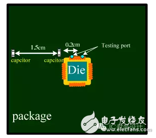
Figure 14 Distance between capacitor and test point
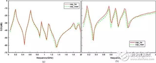
Figure 15 Distance between different capacitors and test points | S21 | Simulation results
It is known from the simulation results that when the capacitor cannot be placed near the noise source due to the package structure or winding problem, we can reduce the influence of noise by reducing the thickness of the Pkg power layer.
Fourth, the conclusion
Finally, we summarize the suppression of noise in high-speed digital circuits. First, the ideal position of the decoupling capacitor is placed on the Pkg; although the ESR increase can flatten the pole, it will also cause the resonance frequency to become shallower, the capacitor charging and discharging time will increase, and the function of reducing the power plane impedance will be lost; The increase of the capacitance ESL will speed up the impedance rise after the resonance point, so the lower the ESL, the better. The more the number of capacitors, the better, the capacitor wall can improve the isolation effect; the choice of capacitance value needs to be selected according to the noise frequency band. Value mixing, although this can increase the bandwidth of noise suppression, but it will increase the number of resonance points. If the noise just falls on the resonance point, the effect of superposition may be more serious; the thickness of the PCB power plane has almost no S parameter on Pkg. Influence, but at low frequencies, the thickness of the Pkg layer will affect the noise of the PCB coupling. The thinner the Pkg layer is, the smaller the noise is coupled. The high frequency part is mainly affected by the package. The thinner the Pkg layer, |S21 |The smaller the value.
Displacement sensor, also known as linear sensor, is a linear device belonging to metal induction. The function of the sensor is to convert various measured physical quantities into electricity. In the production process, the measurement of displacement is generally divided into measuring the physical size and mechanical displacement. According to the different forms of the measured variable, the displacement sensor can be divided into two types: analog and digital. The analog type can be divided into two types: physical property type and structural type. Commonly used displacement sensors are mostly analog structures, including potentiometer-type displacement sensors, inductive displacement sensors, self-aligning machines, capacitive displacement sensors, eddy current displacement sensors, Hall-type displacement sensors, etc. An important advantage of the digital displacement sensor is that it is convenient to send the signal directly into the computer system. This kind of sensor is developing rapidly, and its application is increasingly widespread.
Magnetic Dro Scales,Ditron Magnetic Scales,Magnetic Linear Scale,Electronica Magnetic Scales
Changchun Guangxing Sensing Technology Co.LTD , https://www.gx-encoder.com