Abstract: In order to design a DVB_C digital TV with conditional access function, the processing chip with Trident SoC SXL as the core is used. DDR3 SDRAM uses NT5CB64M16DP, SPI FLASH is MX25L4006E, and NAND FLASH is NAND512W3A2D. The method of receiving and decoding digital television program signals by using the built-in digital television tuner realizes full digitization, reduces the interference and loss caused by the digital television signal in the transmission process, and improves the signal quality of the television reception. The user is in the process of using the TV. Only need to use a remote control to save the remote control of the original set-top box, and enhance the convenience and convenience.
Keywords: digital TV; conditional access; set-top box; flash memory
0 Introduction Digital TV involves standards in many fields, including transmission standards (wireless), cable transmission, and satellite transmission. With the rapid development of digital TV broadcasting and the continuous promotion and development of digital TV technology, people's demand for TV not only needs to be in the need of sound and video programs, but needs to obtain more information. Data broadcasting is a new television service business beyond traditional sound and video. The data broadcasting system can bring more functions such as graphics, text, games, data downloading, and online upgrade to users. There are many TV users in China. Therefore, researching data broadcasting technology and developing a data broadcasting system that conforms to regional characteristics has far-reaching significance for improving China's informationization level. In the next few years, China's digital TV market will be dominated by cable digital TV. Cable digital TV will maintain its dominant position for a long time. The cable digital TV market will occupy the main market of digital TV. China's cable TV network generally uses the European standard DVB-C. This paper introduces a design based on DVB-C digital-analog integrated digital TV with CA function.
1 System composition and hardware design DVB-C digital TV with CA function uses Trident SoC SXL as the core processing chip, and designs video decoding, data stream MPEG decoding, conditional access CA control and other functions centered on Trident SoC SXL. System hardware mainly includes Trident SoC SXL, DDR3 SDRAM NT5CB64M16DP, SPI FLASH MX25L-4006E, NAND FLASH NAND512W3A 2D, power management chip and so on. The block diagram of the system is shown in Figure 1. This article mainly introduces the video signal input part, the external memory part, and the video signal output part.
This article refers to the address: http://
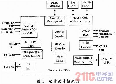
The Trident SoC SXL is highly integrated with a single chip of many components, including H. 264/VCI/MPEG-4/MPEG-2 decoder with integrated ATSC/DVBT/C/Aanalog demodulator, support for DVB_CI+, one PCMCIA card, support for NICAM/BTSC/FM stereo radio, A2 sound demodulation, support for CVBS/ YC separation / HDMI / YPbPr / RGB signal input, integrated MCU, FLASH, Memory controller, can meet the CA-enabled DVB-C digital-to-analog digital TV solution, reducing system cost.
After the digital television signal is encoded and modulated, it needs to demodulate and decode the digitally compressed image and sound signals to generate video and sound signals, and provide high-quality TV programs to the audience through television displays and audio equipment. It is necessary to perform channel decoding on the DVB-modulated digital television signal, and the MPEG-2 transmission stream is divided into video and audio to separate the video, audio and data. If the existing analog TV is to watch digital TV programs, an external digital TV set-top box is needed, which is a conversion device that converts the digital television signal into an analog signal, and then the converted analog signal is input to the analog television display. Its signal mode is that the digitized signal is converted into an analog signal AV output through the set-top box, and is connected to the television by the AV, and converted into digital signal processing in the television, so that the "digital-analog-number" multiple conversion damages the signal.
Digital TV signals usually adopt the structure of "digital TV set-top box + analog TV". The digital TV set-top box converts the digital TV signal into an analog signal conversion device, which decodes and restores the digitally compressed image and sound signals to generate analog video and Sound signal. The modules involved include switching power supply, remote control receiving, button control panel, tuner Tuner, upgrade serial RS 232, flash FLASH, audio and video output interface RCA and conditional access system CA module. The digital-to-digital conversion model of digital TV is essentially a "dual-mode" TV with a built-in digital TV set-top box and the ability to receive analog signals. It does not need to convert the digital TV signal into an analog signal. The switching power supply of the set-top box can be shared with the power system of the TV. The remote control receiving and button control panel also adopts the remote control receiving and button control panel of the TV, and the digital tuner is built into the button. In the main board of the TV, the flash memory FLASH is also shared with the flash memory in the television, and the decoded digital audio and video signals do not have to be reconverted into analog signals and output through the RCA interface. The Trident SoC SXL highly integrated chip meets the "digital-to-digital" conversion model with CA functionality. The need for DVB-C digital-to-analog integrated digital TV design.
1.1 Video signal input design The receiving tuner, generally called Tuner, mainly performs QAM analog demodulation on the RF signal and downconverts the signal to the IF signal. The down-converted intermediate frequency signal passes through the channel decoder chip for channel processing, and can output parallel or serial TS stream signals conforming to the DVB interface standard. SXL can implement data stream processing for input, including demultiplexing, decompressing, descrambling, synchronizing, verifying, and buffering of data streams. The interface block diagram of SXL and TURN BOARD is shown in Figure 2. SXL demultiplexes the transport stream, separates the independent program PES stream and service information such as SI, and then demultiplexes the program PES stream to separate the ES stream of video, audio and data. MPEG-2 mainly includes two parts of video decompression and audio decompression. They decode the compressed video stream and audio stream separately according to the MPEG-2 decoding algorithm, thereby obtaining normal video data and audio data streams.
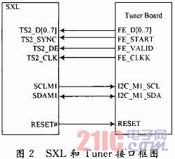
Figure 2, TS2_D[0. . 7] for the data input pin and FE_D[0. . 7] Connected to realize the transmission of 8-bit data signal data. TS2_SYNC is connected to FE_START and is a frame sync signal. TS2_DE is connected to FE_VALID and is a data valid signal. TS2_CLK is connected to FE_CLK and the clock signal is transmitted by data stream. SDAM1 is connected to I2C_M1_SDA to realize data transmission of I2C communication. SCLM1 is connected to I2C_M1_SCL to implement the clock signal for I2C communication. RESET# is connected to RESET to implement reset control. The frame synchronization signal corresponds to the sync byte 047H of the TS packet, and the TS2_DE signal is used to distinguish the length of the TS packet from 188 B or 204 B. When the TS packet length is 188 B, the TS2_DE signal is always high and all signals are synchronized with the clock signal.
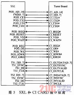
The conditional access CA system is a comprehensive system that integrates data encryption and decryption, scrambling and descrambling, smart card and other technologies. It also involves information management technologies such as user management, program information management, and charge management. Authorization management and reception control of digital television broadcasting services. The interface block diagram of SXL and CI CARD is shown in Figure 3. Figure 3, TS2_D[0. . 7] Data pin and CI_INDATA[0. . 7] Connected to implement encrypted data input to the CA card. TS2_SYNC is connected to CI_INSYNC and is a frame sync signal. TS2_DE is connected to CI_ INVALID and is a data valid signal. TS2_CLK is connected to CI_INCLK, the clock signal for data stream transmission. TS1_D[0. . 7] Data pin and CI_OUTDATA[0. . 7] Connected, the decrypted data is input to SXL. TS1_SYNC is connected to CI_OUTSYNC and is a frame sync signal. TS1_DE is connected to CI_OUTVALID and is a data valid signal. TS1 _CLK is connected to CI_OUTCLK, the clock signal for data stream transmission.
The core of conditional reception is the control of the control word CW transmission. In the digital television system adopting the MPEG-2 standard, there are two data streams related to the program stream condition receiving system: Entitle Control Message (ECM) and EntitleManage Message (EMM). The CW encrypted by the service key SK (Service Key) is transmitted in the ECM, and the ECM also includes program information such as program source, time, content classification, and program price. The CW-encrypted SK is transmitted in the EMM, and the SK is subjected to encryption processing by the user's personal distribution key PDK (Personal Distribute Key) before transmission, and the EMM also includes address and user authorization information.
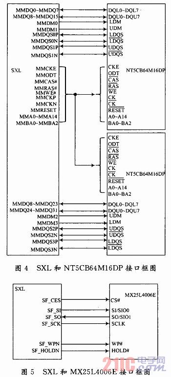
1.2 External Memory Design In this system, the selected external memory is two DDR3SDRAM chips, one SPI FLASH chip and one NANDFLASH chip. In this system, two 1 GB DDR3 SDRAMs from Nanya Technology Nanya are used as main memory, model number NT5CB64-M16DP. The interface block diagram of SXL and NT5CB64-M16DP is shown in Figure 4.
Among them, CK and ![]() It is a clock pin through which the chip clock is input.
It is a clock pin through which the chip clock is input. ![]() Latch for row address,
Latch for row address, ![]() Latch for column address,
Latch for column address, ![]() For write enable, these three pins specify the input command. A0 ~ A14 is the address bus, the row address in the chip is A0 ~ A12, the column address is A0 ~ A9, of which A10 is the automatic pre-charge flag, A12 is the sudden mutation flag.
For write enable, these three pins specify the input command. A0 ~ A14 is the address bus, the row address in the chip is A0 ~ A12, the column address is A0 ~ A9, of which A10 is the automatic pre-charge flag, A12 is the sudden mutation flag. ![]() It is system reset signal control, CKE clock enable control, used for internal clock, device input buffer, external drive.
It is system reset signal control, CKE clock enable control, used for internal clock, device input buffer, external drive. ![]() At reset, keep at least 100 ns low; CKE is
At reset, keep at least 100 ns low; CKE is ![]() After 10 ns is released, the low level is started. After CKE is kept low for 500 μs, active is high, and DRAM starts to initialize internal state.
After 10 ns is released, the low level is started. After CKE is kept low for 500 μs, active is high, and DRAM starts to initialize internal state.
The unit uses 1 GB of DDR3 SDRAM, so select BA0 and BA2 pins to select 8 groups in the chip. DQL0~DQL7 and DQU0~DQU7 are bidirectional data bus pins that support data transmission of 16 widths. When the DQS performs a write operation, the data is output to the chip; when the DQS performs a read operation, the data of the chip is input to the SXL. The differential control signal MMDQS1 is used for MMDQ8~MMDQ15, and the differential control signal MMDQS0 is used for MMDQ0~MMDQ7. The differential control signals LDQS and MMDQS0 are connected, the LDQS corresponds to the DQL0 to DQL7 data, the differential control signal UDQS is connected to the differential control signal MMDQS1, and the UDQS corresponds to the DQU0 to DQU7 data. LDQS and UDQS are low and high data strobes, respectively.
SPI (Serial Peripheral Interface) means a serial peripheral interface. The SPI FLASH selected in the system is Wanghong Electronics' MX25L4006E, which is a 4 MB memory with 128 sectors, 4 kB per sector; it can be divided into 8 blocks, each block size is 64 kB. The power of the flash memory is 3.3 V. The interface block diagram of SXL and NAND512-W3A2D is shown in Figure 5.
In Figure 5, the CS# pin is connected to the SF_CES pin, and the slave device enables the signal to implement the chip select function. The SI/SIO0 pin is connected to the SF_SI pin for data output to the serial data master and slave data input. The SO/SIO1 pin is connected to the SF_SO pin for data input to the serial data master and slave device data output. The SCLK pin is connected to the SF_SCK pin, and the clock signal is generated by the master device. The SPI serial clock pin SCLK is used to control the data transfer between the master and the slave. Starting from the host to send the start transmission signal, the data to be transmitted is loaded into the 8-bit shift register, and 8 clock signals are simultaneously sent out from the SF_SCK pin. Under the control of the SF_SCK signal, the 8-bit shift register is in the host. The data is sent from the SF_SI pin in turn to the slave's SI/SIO0 pin to its 8-bit shift register. During this process, the slave's data is also routed through the SO/SIO1 pin to the host. The WP# pin is connected to the SF_WPN pin to control write protection. The HOLD# pin is connected to the SF_HOLDN pin. When it is low, it means that the serial communication is suspended, and the write operation, program, and erase process are not stopped.
Micron's NAND FLASH selected in the system is NAND512W3A2D, which is a 512 MB memory, each page is 528 B (512 + 16 spare), and each block is 16 KB + 512 B spare bytes. The eight I/O pins are address multiplexed, which reduces pin count and facilitates system upgrades. The flash power supply is 3.3V. The interface block diagram of SXL and NAND512W3A2D is shown in Figure 6.
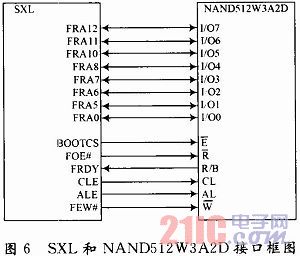
In Figure 6, I/O0~I/O7 are data input/output pins, which are connected to FRA0, FRA5~FRA12 pins for data transmission. I/O pins are used to input commands, addresses, and data. They are also used to output data during a read operation and are locked in The rising edge of the pulse.
The pin is connected to the BOOTCS pin for chip select function.
The pin is connected to the FOE# pin to control the serial data output.
The pin is connected to the FWE# pin to control the write operation to the I/O port. The command, address and data are locked.
The rising edge of the pulse.
The output pin, connected to the FRDY pin, indicates the state of operation of the device. When low, it indicates that a program, erase or random read operation is in progress and returns to a high state after completion. The AL pin is connected to the ALE pin to implement the address lock of the input command. When AL is high, the address is locked.
The rising edge of the pulse. The CL pin is connected to the CLE pin to implement a command lock for the input command. When CL is high, the address is locked.
The rising edge of the pulse.
2 System software design Digital TV is a typical application of embedded system technology in consumer electronics. In an embedded system, the hardware is at the bottom of the system, and the software controls it on it. Digital TV hardware is designed into a number of independent modules, each with relatively independent functionality. These modules can be divided into high frequency head, conditional access, channel demodulator, demultiplexer, host programming interface (master controller), audio decoder, video decoder, OSD display control, graphics processor and so on. In addition, there are some simple modules, such as: infrared remote control, panel button control, LCD display, serial communication port and so on. Audio and video decoders and demultiplexers These relatively complex modules are usually designed as a single RISC DSP processor in hardware. These separate RISC processors use the combination of hardware and software. The hardware uses the DSP architecture, and the software is driven by microcode. The microcode is loaded by the host programming interface after the system is booted.
The software workflow of digital TV is as follows: The source program of digital TV is loaded in the FLASH ROM. After power-on, each chip performs a power-on reset, and the main control CPU loads and runs the program from the FLASH ROM. The program first completes the hardware and software initialization, including clock initialization, system memory initialization, front-end demodulation initialization, and audio and video decoding register initialization, and establishes multiple work processes. The multi-process mode enables the master CPU to process multiple workflows simultaneously and perform communication control between processes. After the system is initialized, the user selects the channel through the remote control, and the channel selection interface is displayed through the OSD. The master CPU responds to the remote command and sets the tuner through the I2C bus, so that the tuner outputs the high frequency signal from the antenna to the intermediate frequency signal. After the IF signal is processed by the channel demodulator, the TS stream is output. The PID filter in the main control CPU implements TS stream demultiplexing, and sends the related ES or PES stream to the audio and video decoder respectively, and finally outputs the audio and video signals. The program information in the TS stream is parsed and stored, and the user queries the menu through the OSD to learn related program information. For a multi-program composite TS stream, the user can also specify to view a specific program in the TS stream through the program guide EPG.
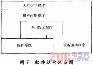
Embedded systems have a real-time operating system. The software system of the video device has higher requirements on real-time performance. The tasks to be completed by the system include: accepting user operations, setting the working status of the tuner, searching for PSI, SI table, demultiplexing, conditional reception, and searching program guide (EPG). Wait. In addition to the real-time operating system, the most complex module in the system is the device driver. The driver layer is the link between the software system and the hardware system. The application service program layer mainly includes a FLASH partition management module, a database management module, and a TUNER management module. The application service module operates by providing a call service to various independent application modules at the same time. Sometimes several application modules are called, and each application module is independent, and the performance of each application module directly depends on the performance of the service call module. The user application layer is the main part of the user application software and is also a major part of software development. The implementation of all upper-level functions related to digital television is done at this level, such as regarding user interface, user information input/output control, program search, program play, analysis processing of program information, and management of program operations. The human-computer interaction program layer includes user API functions, and the user performs frequency point setting, search program, interface for channel selection operation, and the like.
3 Conclusion The system establishes a “digital-to-number†conversion model based on the digital TV signal flow, which will be used as a data conversion model for system design. It is a digital signal that directly demodulates the digital signal through the digital tuner and inputs it to the digital processor in the TV to process the display. It does not need to be demodulated and decoded by an external set-top box, and the whole process can be digitized. At the same time, it is fully built-in, avoiding messy wiring, saving space and cost. The prototype developed in this paper has been verified by experiments and its effectiveness and practical value, and has been put into small batch trial production, which has a good prospect of popularization and application.
Power System Optical Fiber Cable
Simplex Cable,Power System Optical Fiber Cable,Optical Fiber Cable,Large Number Of Cores
Shandong Qingguo Optical Fiber Co., Ltd. , https://www.qgfiber.com