Modern engineering has more opportunities than ever to integrate multiple printed circuit boards and multiple subsystems. To be straightforward, you can't have a single board for a slightly more complex electronic product or system. A complete electronic product generally requires several PCB boards, such as power board, signal input module board, central processing unit module board, core control board, signal output amplifier board, drive board, analog signal part board, digital signal part board. ...and so on and so on. Is it easy for an electronic engineer to do so many things? !
Let me have a little sorrow.
What kind of stuff is included in this picture at the beginning of this article?
Above a PCB board
The following PCB board
Board-to-board connection device
Base below the board
Shell on the board
All these things you see in your eyes are in one project! In a project! In a project!
What is the current state of PCB design routine?       From a few years ago to the present, I often receive questions from customers: Can one of your projects only correspond to one PCB board? Can I import different parts of the schematic into different PCB boards?
Every time I replied: Sorry, a project can only correspond to a PCB board. No matter how many drawings are in your schematic, only one brain can be imported into one PCB. Then I feel a little embarrassed, I can't solve the customer's needs, help the customer to get rid of the cumbersome steps, and focus on the development itself.
As we all know, Altium has always been to solve the troubles of customers at hand, to help customers turn their energy to the perfect design itself, and to launch customer satisfaction works as their responsibility. For decades, we have collected all kinds of requirements from customers, and upgraded and upgraded software tools, trying to make Altium Designer the top equipment and powerful tool for engineers on the design road.
Simpler application   Then, the current status of PCB design is like this.
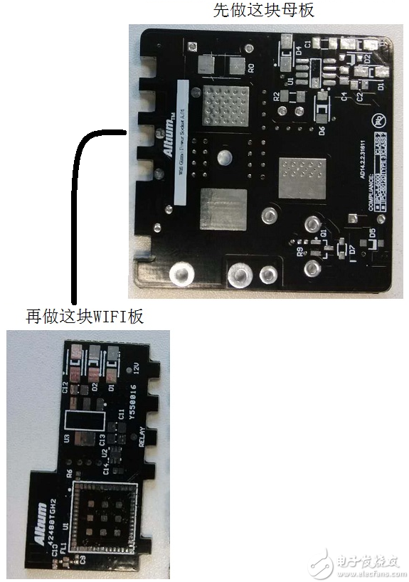
For example, what is to be done is a WIFI-connected IoT small product, a smart socket. The mobile phone can be remotely controlled by the mobile phone, and the home air conditioner, washing machine, television, rice cooker, oven and the like can be remotely controlled.
So for a simple point of application, or a person can stand alone, the following process you must be familiar with.
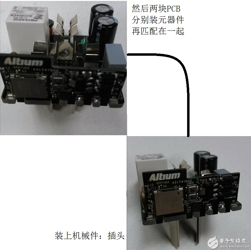
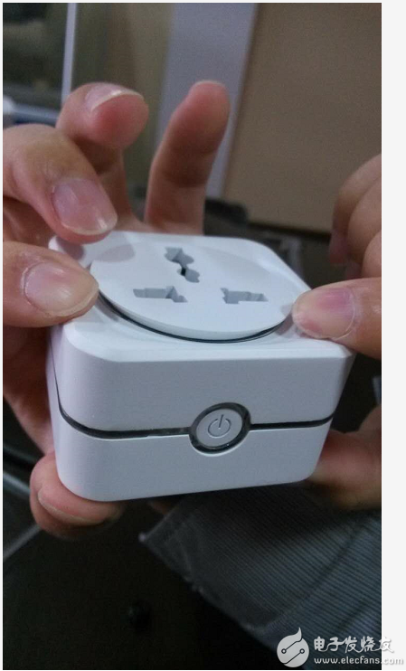
       At this point, the electronic part of the entire electronic product is basically finished. Next, design the mechanical part of the housing of the socket. Take the mechanical part of the designed casing and process it to check the fit. As shown below.
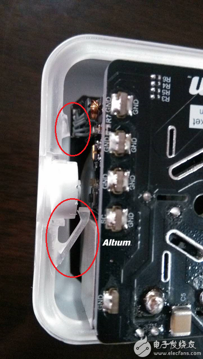
     The smart socket is then assembled with the mechanical housing part of the small product and the electronic combination. If there is no perfect match once, there will always be problems like this. For example, as shown in the figure below, the mechanical housing part originally made two plastic parts of the photosensitive head. During the installation process, the lower photosensitive head is OK, but the upper part of the circuit board is broken! Broken! Broken!
      A simple system is generally the same person to handle, and there are a number of requirements for each board in my heart. Although it is necessary to design, proof, install, test, and cooperate, but how to cooperate with each board. Links can be saved.
However, for the application of complex systems, it will add more communication between the various boards between the PCBs. What is the connection between the board and the board? Which connector is used to connect? If these data are not relying on software but human communication, it is easy to have collisions and errors in information, which leads to the continuous revision of the program.
For example, the following example is about the solution of electrical equipment in IoT applications (kitchen appliances project). The project we are going to do is dedicated to building kitchen appliances for smart IoT connections. By connecting the kitchen smart food machine to the Internet of Things platform, users can control, operate and manage the machine through mobile phones, Ipad and other intelligent electronic terminals or even web pages.
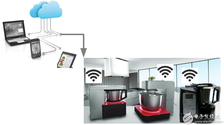
      The project solution integrates the following five major technologies:
Control panel hardware PCB design,
Wifi communication access module design,
Embedded software development,
Smart terminal Android system and IOS system APP design,
Cloud server platform application development
The approximate structure of the machine is as follows:
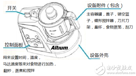
    The electronics-related hardware components that need to be designed are:
Man-machine interface board (mechanical part, ECAD-MCAD collaboration required)
Power supply PCB board (Power Board)
Control board PCB (Control Panel)
Wifi interface board (Wifi Board)
Then the division of labor and cooperation, some mechanical engineers design the mechanical part of the man-machine control interface board, the button position of the board, the LCD display position, etc. must be in one-to-one correspondence with the control board PCB.
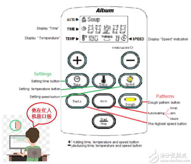
Here are some people who are busy with the interface board (mechanical part, need ECAD-MCAD collaboration)
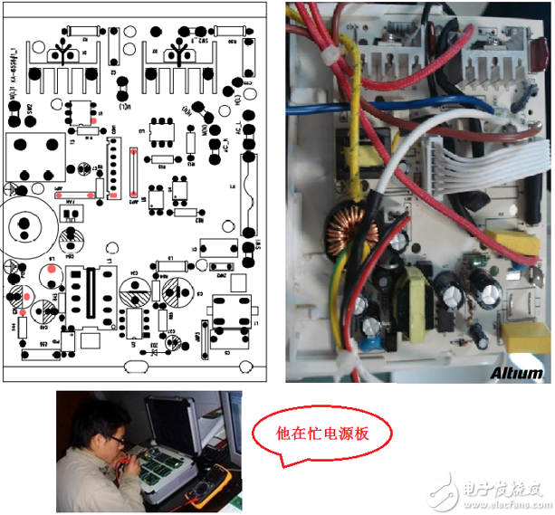
Someone is busy with power supply PCB board (Power Board)
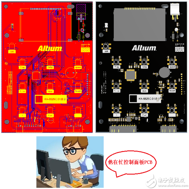
Someone is busy controlling the motherboard PCB (Control Panel)
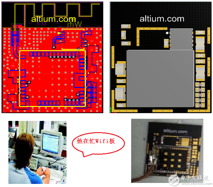
Someone is busy Wifi interface board (Wifi Board)
    Then after completing their own modules, when they were integrated together, the problem came.
How to control the interface between the motherboard PCB and the power supply PCB (Power Board)?
How to connect the interface between Wifi interface board and control board PCB?
How does the signal communication between the Wifi Board and the control board PCB work?
Where does the power board need to be changed when controlling the motherboard PCB, or where does the power board need to be changed?
Need to coordinate the software firmware between the Wifi Board and the control board?
Is there a problem with the electromechanical ECAD-MCAD coordination between the human interface board and the control panel?
Next, the officers can appreciate some of the work of communication and collaboration between the heads of the design modules.
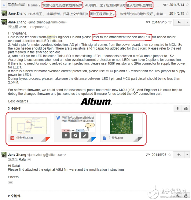
These indirect plug-ins for debugging are carefully defined between the boards and marked out to avoid errors!
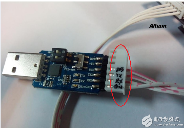
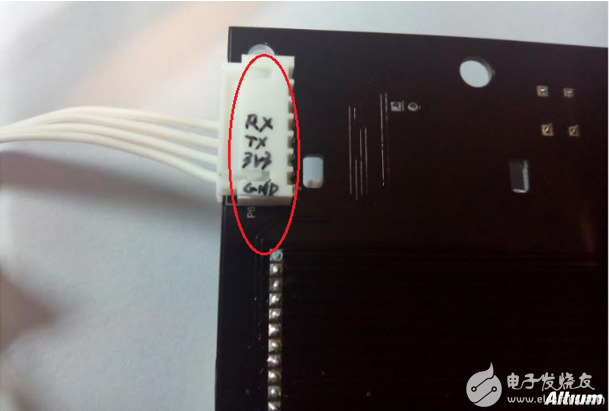
      Then in the process of proofing between the boards, debugging, joint debugging, I have to change this, you have to change that, to communicate back and forth by phone. Take a part of the message as follows:
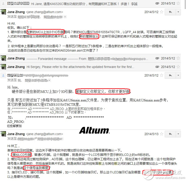
      Then the documents are sent and sent, plus various explanations, requests, communication, and coordination of relevant designers in each part to maintain the sharing and consistency of information.
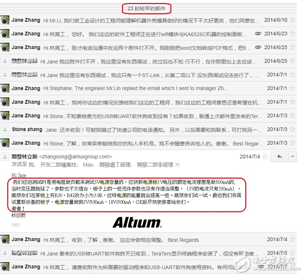
      As shown below, there are up to 30 emails back and forth for a certain problem, which consumes a lot of time for communication, update and iterative process.
      After the completion of the debugging of all the PCB boards in the project (often need multiple proofing, debugging, multiple replacements), the electronic part of the product design needs to be placed in the machine for electromechanical coordination and testing.
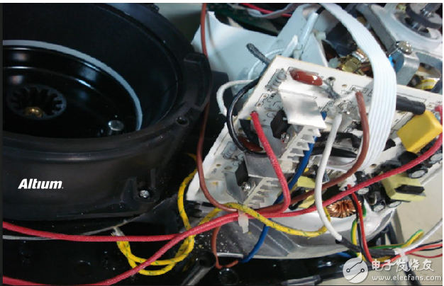
The following is the power board placed in the machine, all kinds of chaos, cable, connector dazzling! ! !
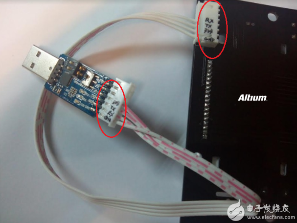
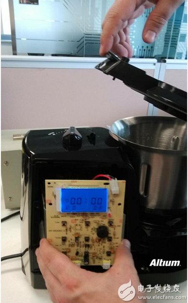
     The following is the connection between the control panel PCB and the machine.
       In summary, the problems and troubles of this series are the huge time and energy required for communication, integration and joint debugging between independent PCB boards. So, if all of these discrete PCB boards (including the schematic design files of each board, PCB files), and the management of the connection between each PCB and PCB board are in the same project, what kind of experience would it be? Open Altium Designer18 and you will find that the world really changes too fast.
Watch Screen Protector features a stretchable and retractable TPU Screen Protector that resists air bubbles and fingerprints on your device's screen and provides maximum protection for your device from scratches. The Hydrogel Film repairs screen scratches on its own and is ideal for curved curved screens.
Full Coverage: The soft material matches the edges of the watch screen well. Full coverage provides better protection and looks very discreet.
Oleophobic and waterproof: The oleophobic waterproof transparent layer can prevent the residue of sweat and grease, resist fingerprints, and keep the phone screen as new as ever.
Sensitive touch: only 0.14mm thick ultra-thin protective layer will not interfere with touch screen commands, your touch screen can still operate 100% normally.
If you want to know more information about Smart Watch Screen Protector products, please click the product details to view the parameters, models, pictures, prices and other information of Watch Screen Protector products.
Whether you are a group or an individual, we will do our best to provide you with accurate and comprehensive information about Watch Hydrogel Screen Protectors!
Watch Screen Protector, Watch Hydrogel Screen Protector,Smart Watch Screen Protector,Watch Protective Film,Apple Watch Screen Protector,Watch Screen Protector Cover
Shenzhen Jianjiantong Technology Co., Ltd. , https://www.jjtscreenprotector.com