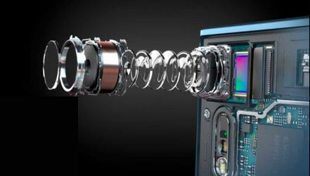
In order to accelerate image data processing, the industry has developed an embedded dynamic random access memory (DRAM) in complementary metal-oxide-semiconductor (CMOS) image sensors and introduced a three-layer stacked CMOS image sensor equipped with DRAM. SONY was first released. The manufacturer of this product, this model IMX400 three-layer stacked sensor (Exmor RS) is designed for smart phones and build.
SONY Stacked CMOS Sensor Element
Sony's Xperia XZ Premium and Xperia XZ's flagship smartphones feature a Motion Eye camera module with 960 fps update rate.
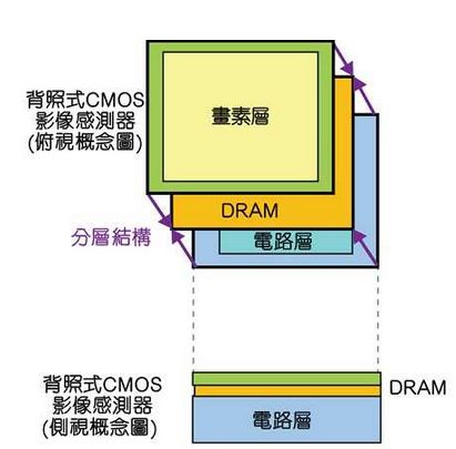
The three-layer stacked CMOS image sensor (CIS) is mounted face-to-face on the DRAM, allowing the DRAM to interface with the video signal processor (ISP).
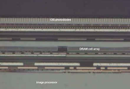
Cross-section of a Sony 3-layer stacked CMOS image sensor
Sony uses dual analog/digital converters (ADCs) in its earlier 19Mp image sensor to digitize pixel data. Today, the company uses a 4-layer ADC architecture to increase read speeds while also improving processing capabilities. DRAM is used to temporarily store high-speed data and then output it at the optimal rate of the sensor interface. The design enables it to read 19.3 million pixels of still images in 1/120 seconds, and achieve 1,000fps in video mode, which is 4x and 8x higher than previous still and dynamic videos. speed. Sony can be said to once again push the capabilities of mobile camera to the limit.
Sony Newly Develops 3-layer Stacked CMOS Image Sensor with DRAM
3D stacking technology
The 3D stacking technology is a chip or structure with different functions. Through micromachining techniques such as stacking technology and via interconnection, it forms a three-dimensional integration and signal connection in the Z-axis direction and a wafer-level, chip-level, silicon cap package. Three-dimensional stacking processing technology, such as packaging and reliability technology, for micro-system integration, advanced manufacturing of system-in-package (SiP/SoP) developed after on-chip system (SOC), multi-chip module (MCM) new technology.
Microelectronics modules have implemented 3D wafer-level packaging (WLP) system-in-package (SiP) technologies, such as CIS RF modules, MES packages, and standard device packages, have been in volume production, and began the 3D TSV stacking era in 2009. With the advent of 3D TSV Stack Era, modular chips, flash memory and DRAM are stacked to achieve enhanced memory capacity.
The main form and classification of 3D stacking
There are various methods based on 3D stacking, mainly including: chip-to-chip stacking (D2D), chip-to-wafer stacking (D2W), and wafer-to-wafer stacking (W2W).

The D2D stacking mode is the main interconnection mode of the current System-in-Package (SiP) mode. This stacking method mainly utilizes the wire bonding method to realize the interconnection between chips in the 3D direction, as shown in (a). D2D mode can realize 3D stacking and improve system integration. However, due to the main use of wire bonding methods to interconnect, the system integration is further limited, and the parasitic effects of the leads are introduced to reduce the performance of the 3D system.
The D2W stacking method uses chips to implement 3D stacking corresponding to the functional positions of the wafers, as shown in (b). This method mainly uses the flip-chip (flip) and bump (bulb) bonding methods to implement the chip and The interconnection of the wafer electrodes, this method has higher interconnection density and performance than the D2D method, and in conjunction with a high performance flip-chip bonder, high production efficiency can be achieved;
The W2W stacking method uses wafers and wafers for bonding to achieve 3D stacking. During the wafer bonding process, signals are interconnected using TSV. As shown in (c), this method has high interconnection density and low cost. The advantages of wafer-level packaging (WLP) can be achieved at the same time, and the hybrid integration of AD, I/O, and sensors can be realized.
For the D2W and W2W stacking methods, the W 2W method is the most efficient from a production efficiency point of view. However, from the viewpoint of yield, the D2W method can achieve the stacking between the qualified chips (KGD) through screening, so the finished product The rate is higher; while the W2W method cannot be implemented through prior screening, it will seriously affect the yield of the stack.
For the W2W stacking method, the yield of the chip and the 3D stacking process must be strictly controlled. Otherwise, as the stacking layer number increases, the yield will decrease significantly. For a stacking process that requires 3 layers, wafer yield and stacking yield must be controlled at more than 98% to achieve a 90% or more 3D stacking yield.
Interlayer interconnection technology - TSV
From the perspective of the development trend of microelectronics technology, 3D stacking technology based on TSV technology will be an inevitable trend for the development of microelectronics technology, but it also faces many technical challenges, such as TSV technology, super-laminate processing technology (temporary bonding, thinning Etc.), heterogeneous bonding technology, interlayer alignment technology, etc. Among them, TSV technology is the most critical.
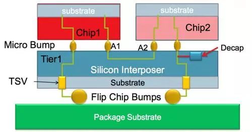
Through-silicon-vias (TSVs) will provide interconnection between layers of chips in advanced 3D IC designs by creating verticals between the chip and the chip and between the wafer and the wafer. Turn-on, the latest technology for interconnecting chips. Unlike previous IC package bonding and bump overlay technology, TSV enables the chip to stack in three dimensions with the highest density and smallest form factor, and greatly improves chip speed and power consumption.
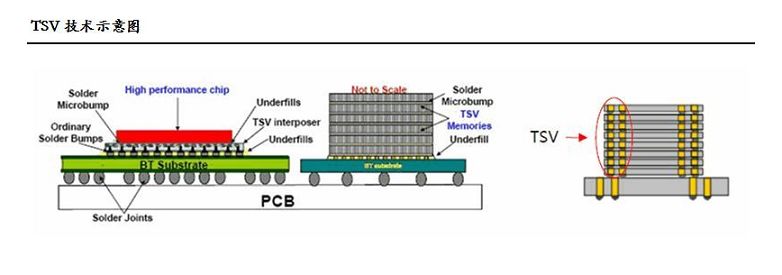
Stacked Devices Using Through-Silicon Via Technology (TSVs)
TSV is different from the vias currently used for multilayer interconnections. On the one hand, TSV vias typically have a diameter of only 1 to 100 μm, a depth of 10 to 400 μm, and high-density mixing of integrated circuits or other multi-function devices. The integration offers the possibility; On the other hand, they not only need to penetrate the various materials that make up the laminated circuit, but also need to penetrate the very thick silicon substrate, so the etching technology for the through-hole has higher requirements. A variety of 3D integration solutions currently being considered by manufacturers also require a variety of sizes of T SVs to work with. Plasma etching technology has been widely used in deep silicon etching processes for memory and MEM S production. It is also very suitable for the manufacture of TSV.
The use of 3D stacking technology to realize micro-systems is an inevitable trend for future development and is an inevitable choice to break through the development of Moore's Law. Among them, the use of MEMS technology to realize TSV interconnection is the core technology of this technology and must be focused on solving and breakthroughs.
Stylus Pen Tip,Stylus Pencil Tip,Carbon Fiber Pen Tip,Carbon Fiber Stylus Pen Tip
Shenzhen Ruidian Technology CO., Ltd , https://www.szwisonen.com