 Resistance is the most commonly used electronic component. Good steel needs a lot of temperament, good resistance also requires repeated fire exercises. Now let us take the thick film resistor as an example to talk about how the resistor is made.
 The production process of thick film resistors generally needs to undergo the following processes: substrate grooving, electrode printing and sintering, resistance printing and sintering, primary glass body formation, resistance adjustment, secondary glass body formation, primary substrate cutting, terminal electrode formation, and substrate secondary Cutting, end-making, screen printing and packaging.
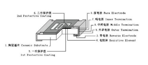
1. The substrate with grooved thick film resistors is the carrier that carries the resistors. Generally, the substrate is made of high-purity aluminum oxide ceramic, which is often referred to as corundum porcelain or high-alumina porcelain, and also employs yttrium oxide or aluminum nitride ceramics as the substrate. However, the latter two are generally used in high-end, high-power resistors. It is common to use corundum ceramic substrates.
The basic requirement of the resistor to the substrate is to have a higher thermal conductivity, a smaller thermal expansion and, in addition, a higher mechanical strength. These are the basic requirements for ensuring high-quality resistors.
Many resistance manufacturers often purchase ceramic substrates. Because of the high hardness of ceramic substrates, lasers or electric sparks are first used to form criss-cross grooves on the substrate.
2. Electrode Printing The electrodes that need to be printed at this time are the surface electrode and the back electrode in the figure. The two electrodes are printed on the substrate using a screen printing method. After printing is completed, the electrodes are firmly adhered to the ceramic substrate after sintering.
3. Resistor printing and sintering resistors are also printed on a ceramic substrate by means of screen printing. The yttrium oxide paste is printed on a ceramic substrate, and then put into a sintering furnace for sintering.
4. In order to protect the resistor and also to adjust the resistance of the primary glass body, a screen printing method is used to print and sinter a layer of glass material on the resistor body. (One layer of protection in the picture).
5. Although the resistor body is sintered on the substrate after the resistance adjustment, the resistance value may also be out of tolerance. Therefore, the resistance of the resistor body needs to be adjusted. This method adjusts the resistance value by measuring the resistance while cauterizing the resistor body with a laser. Until the resistance reaches the design requirements.
6. After the secondary glass body is formed by laser trimming, the primary glass body of the resistor will also be burned by the laser. In order to protect the exposed parts, it is necessary to sinter a layer of glass on the resistor. This layer of glass is called a secondary glass body. Some manufacturers of secondary glass body, not using glass, but the use of resin material, its purpose is still to protect.
7. Before the substrate is cut to this step, all the resistors are still on the same substrate. Although in the electrode printing process, the surface electrode and the back electrode have been produced. However, there is no communication between the top electrode and the bottom electrode. Therefore, in this process, the substrate is first cut in the longitudinal direction.
8. After the terminal electrode forming substrate is cut in the longitudinal direction, the terminal electrodes of the communication surface electrode and the back electrode are formed on the side surface of the substrate.
9. After the secondary cutting of the substrate is performed, the substrate is cut transversely. At this time, one of the resistors appears.
10, although the end of the end of the electrode production is completed. However, since the terminal electrode is thin, and in order to ensure solderability, it is necessary to make a tip for soldering. This type of tip is generally a three-layer structure. The innermost surface is the terminal electrode. Then, in order to improve the soldering resistance, the rear end electrode is plated with nickel as an intermediate electrode. Finally, a layer of tin with good solderability is plated.
11. Screen printing and packaging The final resistance is printed on the resistance and it is packaged into the warehouse.
The above is the basic production process of thick film resistors. For thin film resistors, the main difference is in step 3. The thick film resistors are printed on the substrate by screen printing a yttrium trioxide paste, and the thin film resistors are deposited on the substrate by evaporation or sputtering by means of evaporation or sputtering.
As you can see from the above, the production of a small resistor requires many processes. Only strict control of the processes can ensure that the resistors are produced with high quality.
DG200 Double Roller Granulator
Dry Roll Press Granulator Co., Ltd. , http://www.nspelletmill.com