Yang Zhenjia, Liu Yingjie, Deng Fangfang, Xie Hua, Li Li, University of Electronic Science and Technology of China
Keywords: High-speed signal acquisition, Fibre Channel, High-speed transmission, FPGA, CPCI, DDR2 SDRAM
With the rapid development of modern electronic information technology, the bandwidth for processing signals has become higher and higher. In order to meet the need for accurate and real-time processing of high-frequency period and transient aperiodic signals in a wide frequency range, a high sampling rate, high resolution signal acquisition module is necessary to complete fast sampling of high-speed and complex signals. , storage and transmission. The high-speed signal acquisition storage and optical fiber transmission system proposed in this paper uses Altera's Stratix IV processing platform, which mainly completes the real-time preprocessing and control of digital signals such as high-speed data flow grouping, wideband digital down conversion, and variable bandwidth channelization filtering. Implementation of DDR2 SDRAM SODIMM memory stick control, complete the local data cache operation; 64-bit CPCI interface, complete with the host computer's communication function; high-speed data transmission of optical fiber. The system has high integration, stable performance and good application prospects.
1 system design
In this design, the data acquisition module uses two 12-bit A/Ds (AD9434BCPZ-500) for data acquisition. The system mainly processes the collected data, including digital down-conversion, FFT conversion, etc., and stores the processed data in 1 GB of DDR2 SDRAM SODIMMs. After acquiring a certain capacity, the data is no longer stored in the DDR2 SDRAM. Wait for the upper computer to read the data in the DDR2 SDRAM memory before continuing to access it. The upper computer reads data through the CPCI interface and performs spectrum analysis, envelope demodulation, and real-time display on the read data. When the operator observes that the data is stable and can be transmitted over a long distance, it sends a start transmission command through the host computer, the transmission path is enabled, and the high-speed fiber transmission part starts to work, thereby starting the high-speed data transmission. To cope with situations where the data transmission rate is greater than the data collection rate, data integration operations are added to the data transmission module, and the integrated data is asynchronously cached to solve the problem of cross-clock domain data. The integrated data is packaged into frames according to the FC protocol standard, 8B/10B encoding, and high-speed parallel/serial conversion. Finally, high-speed serial digital signals are converted to optical signals for transmission via optical modules. The overall scheme of the system is shown in Figure 1.
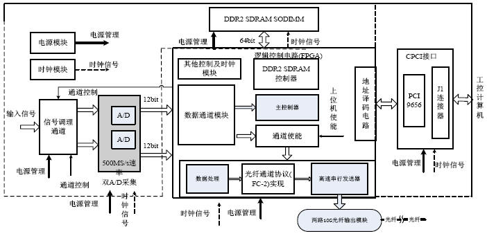
Figure 1 Overall System Diagram
2 main FPGA logic module design
2.1 FPGA logic design overall plan
As shown in Figure 2, the entire system is based on FPGA. The work of FPGA can be divided into two parts: logic control and data transmission. FPGA receives the control command word of the upper computer through PCI 9656, controls A/D acquisition, data transmission work, and coordinates the work of the whole system; At the same time FPGA must upload the data that A/D gathers.
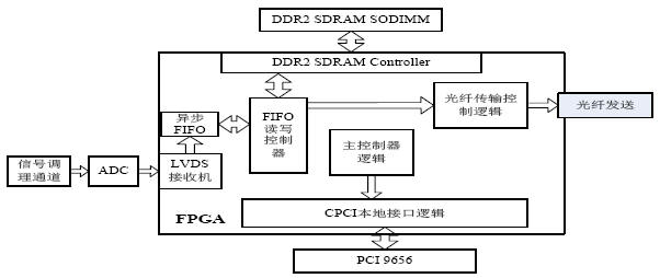
Figure 2 FPGA logic design overall plan
2.2 PCI 9656 Local Interface and System Control Logic Module
First, when the PCI 9656 obtains the write command and write data from the PCI bus, it begins to request the bus control right from the local; after the bus control is obtained, the ADS signal transitions downwards and continues for one cycle of negative level while sending the local write address and Write data, after the write signal is valid for one clock cycle, if the Ready# signal returned by the local bus is low, indicating that the local has received data, PCI9656 will send the next write address and write data; if the signal is high The last write address and data will continue until the signal goes high.
2.3 A/D acquisition data receiving module
The data acquisition card uses a 12-bit AD9434BCPZ-500 chip with a maximum sampling rate of 500 MS/s from TI. The chip's clock at 500 MS/s sampling rate is 500 MHz. In the FPGA, the A/D clock can be used to deserialize the sampled data. To reduce the data input rate, use the 4-times LVDS deserialization method to reduce the data input rate. The output de-serialization clock is 125 MHz. The data width is 48 bit. After de-serializing, the 48-bit parallel data is interleaved with adjacent 12-bit bits. It is necessary to re-arrange and combine them so that the high and low 12 bits are a complete data.
2.4 DDR2 SDRAM Controller and Local Interface Logic Design
2.4.1 DDR2 SDRAM Controller Local Read Logic
When the PCI 9656 reads data in the local DDR2 SDRAM in DMA mode, the module sends a read data request signal local_read_req to the DDR2 SDRAM controller and sends the read address. When the local_rdata_valid signal output by the DDR2 SDRAM controller is valid, it indicates that the read data has been sent out. At this time, these data are latched and sent to the PCI 9656. The local_ready signal is judged. If the signal is valid, the read request can continue to be sent to the DDR2 SDRAM controller; if the signal is invalid, it waits until the signal is valid and then initiates the read request. Until PCI 9656 reads data in empty DDR2 SDRAM.
2.4.2 DDR2 SDRAM Controller Local Write Logic
A/D collected data is first stored in two asynchronous FIFOs, and two FIFOs are used for ping-pong operation. When one of the FIFOs is full, a write DDR2 request is issued locally to the DDR2 SDRAM controller. After receiving the request, the local controller issues a FIFO fixed-depth byte count request, and then returns to waiting for the FIFO empty state. After receiving the null signal, the local controller jumps back to wait for the write state and waits for the FIFO to be full again. This is repeated until the IDLE state is returned after filling a fixed capacity. The state transition is shown in Figure 3.
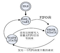
Figure 3 DDR2 SDRAM controller write timing module state transition diagram
2.5 Fibre Transport Mechanism Design Based on FC Protocol
2.5.1 Frame Generation
The composition of the frame includes a starting delimiter, a header, a data payload area, a CRC check bit, and a termination delimiter. The frame generation module completes the assembly process of the corresponding frame at different stages under the control of the state machine. The transmitted frames include PLOGI (login frame), LOGO (logout frame), and data frame. The internal function structure of the frame generation module is shown in FIG.
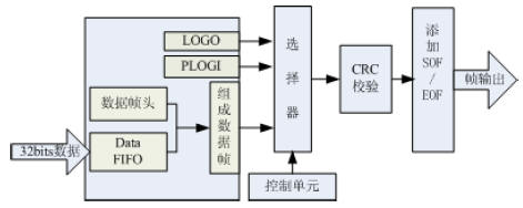
Figure 4 Frame Generation Module
2.5.2 Port Control State Machine
After the system is powered on, it first enters the port initialization state. After the initialization is completed, it enters the IDLE state. If no send command is received during the power-up, the IDLE primitive is sent to fill. When the Send command is received, the system goes to the SEND FLOGI state. The login frame, after receiving the LS_ACC frame, confirms that the login is successful and adds the start delimiter and jumps to the SEND FRAME DATA state. When the Stop command is received, the CRC check bit is added and the end frame EOF is turned to the SEND LOGO state, and is sent in this state. LOGO frame, request logout, return to IDLE state after receiving LS_ACC frame, wait for the next transfer command.
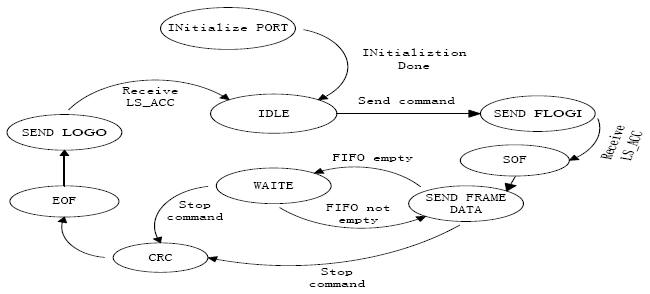
Figure 5 port control state machine transition diagram
3 system debugging and result analysis
This system adopts Stratix IV GX series chip of Altera Company, the design is totally compiled by Quartus II 10.1. According to its compilation report, the realization of the hardware system occupies less hardware resources, which provides sufficient resources for the design of multi-path fiber channel transmission in the future. Because the system has two fiber ports, the self-test mode is used during testing. One is used as the transmission port, the other is used as the receiving port, and only one A/D is enabled locally. Now the 60 MHz IF signal is collected, transmitted and received to the host computer. The host computer performs spectrum analysis and demodulation on the received data. The test results are shown in Figure 6.
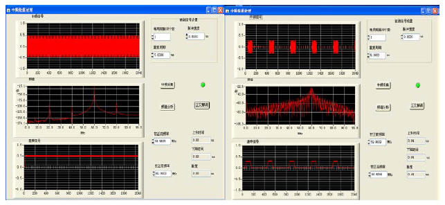
Figure 6-1 Sinewave acquisition at 60MHZ Figure 6-2 Modulation wave acquisition at 60MHZ
It can be seen from Figure 6 that the upper computer shows the signal waveform of the sine wave (modulation wave) received by the receiver, which is consistent with the original data waveform monitored before transmission. Explain that the system can correctly recover the collected signals and basically meet the design requirements.
4 Summary
In this paper, based on the study of the frame structure of the Fibre Channel protocol and the interactive mode of different service types, we refer to the third type of services of the Fibre Channel protocol. Combined with the application requirements of the current automatic test system, we design a high-speed signal acquisition based on optical fiber. Storage and fiber transmission systems. The application of DDR2 SODIMM memory bar and optical fiber transmission technology reduces the system cost, and the system's main data processing, control and transmission protocols are implemented in the FPGA, greatly reducing the system complexity, making the system performance, integration and Stability has been greatly improved, while increasing the flexibility of system design.
Features of LiFePO4 car starter Battery:
Fast charging
Energy saving, 8%~13% automobile fuel saving>8.36%
Low temperature start
Super long life and light weight, 1/3 weight and volum as traditional Lead Acid Battery
Strong current and stable discahrge, instant start quickly, peak discharging current can reach 2300CCA, suitable for autos espacially racing car
Build in BMS, more safety and no fire
The start-stop system has excellent performance
Environmental friendly, not contain heavy metal like Pb
Lithium Car Battery
Car Starting Battery,Jump Starting Battery Pack,lithium car starting battery,car battery replacement,lifepo4 car battery 12v
Starlight Power Industrial Company Limited , https://www.starlite-power.com