The thermal resistance, that is, the resistance encountered by heat in the heat flow path, reflects the amount of heat transfer between the medium or medium, indicating the temperature rise caused by 1 W of heat, in °C/W or K/W. An analogy can be used to explain that if the heat is equivalent to the current and the temperature difference is equivalent to the voltage, the thermal resistance is equivalent to the resistance. Generally, in the application of the LED device, the structural thermal resistance is distributed into the chip substrate, the bonding layer between the substrate and the LED holder, the LED holder, the external heat sink of the LED device, and the thermal resistance of the free space, and the thermal resistance channels are connected in series.
As a new energy-saving luminaire, LED luminaires only convert 30-40% of electrical energy into light during the lighting process, and the rest become thermal energy. The existence of thermal energy motivates us to pay attention to the thermal resistance of LED packaging devices. In general, the higher the power of the LED, the more obvious the thermal effect of the LED, and the problems caused by the thermal effect are also highlighted, for example, the red shift phenomenon of the high temperature of the chip; the permanent damage of the chip due to the excessive junction temperature; the luminous efficiency of the phosphor layer is lowered. And accelerated aging; color temperature drift phenomenon; mechanical failure caused by thermal stress. These directly affect the LED's luminous efficiency, wavelength, forward voltage drop and lifetime. LED heat dissipation has become a huge bottleneck in the development of lamps.
How should I evaluate the heat dissipation level of LED package devices?
Application examples
1. Package device thermal resistance test
(1) Test method one:
In the process of testing the thermal resistance, the general heat dissipation path of the packaged product is a chip-solid layer-support or substrate-solder paste-assisted test substrate-thermal conductive connecting material.
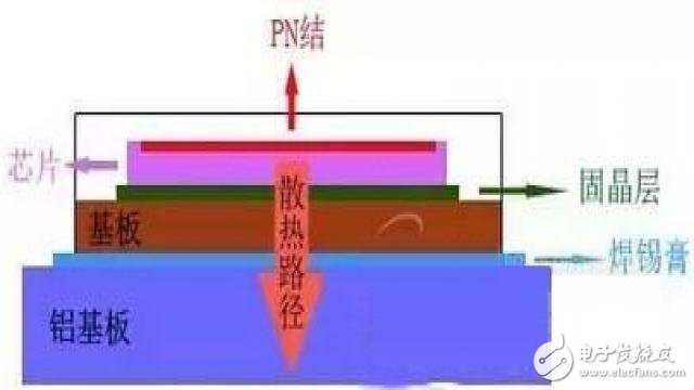
Side structure and heat dissipation path
According to the test, the thermal resistance curve as shown below can be obtained, and the total thermal resistance (the entire heat dissipation path) of the test product can be read as 7.377 K/W. The thermal resistance tested by this method needs to determine the thermal resistance delamination in the curve according to the structure of the test sample, and obtain the accurate thermal resistance of the packaged device. This method is more suitable for SMD package devices.
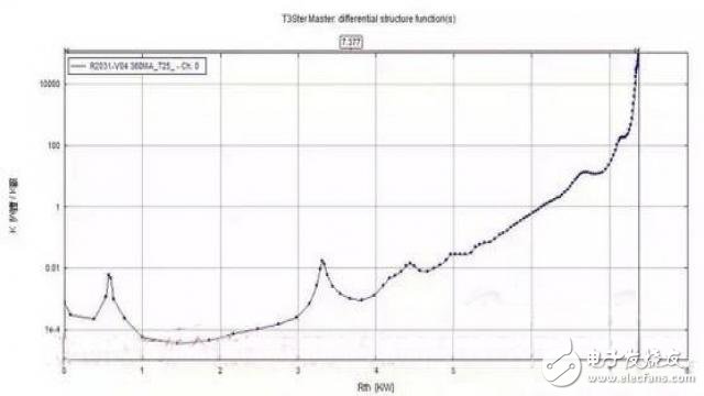
Thermal resistance curve
(2) Test Method 2:
Different from method one, the method needs to undergo two thermal resistance tests, and the obtained thermal resistance can be accurately determined to the device substrate casing without the value of the test substrate.
The difference between the two tests: the first measurement, the device directly contacts the substrate heat sink; the second measurement, the device and the substrate heat sink sandwich the thermal double-sided tape. Since the change of the two heat dissipation paths only occurs outside the device package, the boundary of the two measurements on the structure function represents the shell of the device. The exact thermal resistance of the device can be derived from the curve changes shown below. This method is suitable for COB packaged devices.
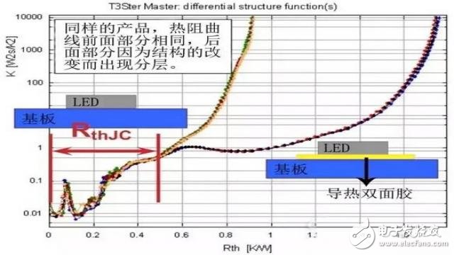
Comparison of thermal resistance curves for multiple tests
(3) Identifying the structure of the device using the structure function
Conventionally, the thermal resistance and heat capacity of the three layers of the chip, the support or the substrate, the test auxiliary substrate or the cold plate are relatively small, and the thermal resistance and heat capacity of the solid crystal layer and the thermally conductive connecting material are relatively large.
As shown in the following structure function, the closer the structure function is to the y-axis, the structure close to the active region of the chip on the actual heat flow path, and the farther away from the y-axis represents the structure farther away from the active region on the heat flow path. . The integral structure function is the heat capacity-thermal resistance function. The flat area on the curve represents the structure with large thermal resistance inside the device and small heat capacity. The steep region represents the structure with small thermal resistance inside the device and large heat capacity. In the differential structure function, the inflection point of the peak and the trough is the boundary between the two structures, which is convenient for identifying the various layers inside the device. At the end of the structure function, its value tends to a vertical asymptote, which means that the heat flow is conducted to the air layer. Because the volume of the air is infinite, the heat capacity is infinite. The x value from the origin to this asymptote is the thermal resistance of the junction to the air environment, which is the thermal resistance at steady state.
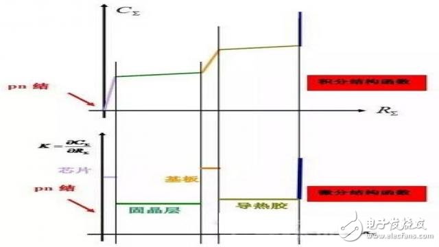
Two structural functions of the thermal resistance curve
2. Defects inside the packaged device
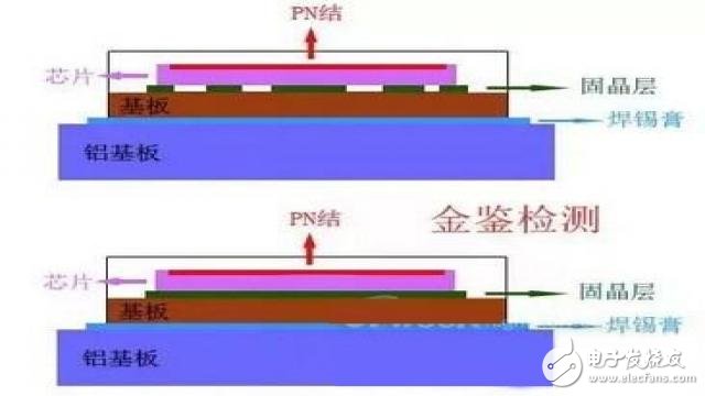
Solid crystal layer internal defect display
Comparing the cross-sectional structures of the above two devices, the solid crystal layer shows significant differences. As shown below, the left side is a normal product, and the right side is a product with a defective solid crystal layer.
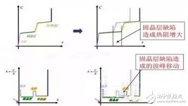
Thermal resistance caused by defects in the solid crystal layer becomes large
According to the above figure, the thermal resistance caused by the defect of the solid crystal layer increases, which affects the heat dissipation performance. The specific degree of influence is related to the size of the defect.
T16 Series Terminal Blocks,Barrier Terminal Connector,Polypropylene Terminal Block,Polyamide66 Terminal Blocks
Jiangmen Krealux Electrical Appliances Co.,Ltd. , https://www.krealux-online.com