This article refers to the address: http://
Abstract: VS1001K is a new MP3 decoder chip produced by Finnish VLSI Solution. The chip contains a high quality stereo digital-to-analog converter (DAC) and headphone driver circuit to support PCM data input. It also has the advantages of small size, low power consumption, simple interface and low price. The pinout, internal structure and main features of the VS1001K are described. At the same time, the function and address of each register in the SCI control interface of VS1001K and the operation method of SDI data interface are introduced. Finally, the application circuit of VS1001K is given.Keywords: MP3 code player VS1001K
1 Introduction
At present, the MP3 audio data compression method used by INTERNET online and portable players has become a recognized industry standard. This method is rapidly popular around the world with its high compression ratio and good sound quality. But in fact, the core of many MP3 players is an MP3 audio decoder chip. VS1001K is a new MP3 decoder chip from VLSI Solution of Finland. The chip contains high-quality stereo digital-to-analog converter (DAC) and headphone driver circuit, which supports PCM data input, and has the advantages of small size, low power consumption, simple interface and low price. Therefore, it is expected to become the chip of choice for the new MP3 decoder.
2 VS1001K functional structure
2.1 VS1001K pin function
The VS1001K is available in two package styles: a 28-pin SOIC dual-row and a 49-pin BGA ball grid array. Figure 1 shows the pinout of a 28-pin SOIC package. The specific function description of each pin is listed in Table 1.
Table 1 VS1001K pin function
| Pin number | Pin name | Features |
| 1 | DREQ | Data request port |
| 2 | DCLK | SDI clock signal input |
| 3 | SDATA | SDI data input |
| 4 | BSYNC | Byte sync signal |
| 5,9,28 | DVDD | Digital power supply |
| 6,10,27 | DGND | Digitally |
| 7 | XTALO | Clock signal output |
| 8 | XTALI | Clock signal input |
| 11 | XCS | Chip select, active low |
| 12 | SCLK | SCI clock input |
| 13 | SI | SCI data input |
| 14 | SO | SCI data output |
| 15~17 | TEST0 | Alternate test port |
| 18,21,25 | AGND | Analogue |
| 19,23 | AVDD | Analog power supply |
| 20 | RIGHT | Right channel audio output |
| twenty two | RCAP | External capacitor access terminal |
| twenty four | LEFT | Left channel audio output |
| 26 | XRESET | Circuit reset terminal, active low |
Table 2 SCI register function
| Register name | Address | Types of | Features |
| MODE | 0x00 | RW | Used to control the operation of the VS1001K |
| STATUS | 0x01 | RW | Status information of the current VS1001K |
| INT_FCTLH | 0x02 | - | Internal registers, generally not used |
| CLOCKF | 0x03 | RW | Control clock frequency and frequency multiplier |
| DECODE_TIME | 0x04 | R | Determine the decoding time (in seconds) |
| AUDATA | 0x05 | R | Sound data |
| WRAM | 0x06 | W | Used to write user program to program RAM |
| WRAMADDR | 0x07 | W | Set the base address for WRAM operations |
| HDAT0 | 0x08 | R | Read MP3 header data |
| HDAT1 | 0x09 | R | Read MP3 header data |
| A1ADDR | 0x0A | RW | Determine the start address of the user application |
| VOL | 0x0B | RW | For volume control, the high and low bytes are left and right channels respectively. The volume range is from 0 to FF, the 0 bit is the largest, and the FF is the smallest. |
| RESERVED | 0x0C | - | Reserved |
| A1CTRL[0] | 0x0D | RW | Used to control user applications |
| A1CTRL[1] | 0x0E | RW | Used to control user applications |
2.2 Internal structure of VS1001K
The VS1001K decoder chip integrates a VS DSP processor, and it also integrates a stereo audio DAC, a stereo headphone amplifier driver, and a program ROM and program RAM. In addition, the VS1001K also has a serial data interface and control interface. Figure 2 is a block diagram of the internal structure of the VS1001K.
3 How does VS1001K work?
The VS1001K accepts external microprocessor transfers via two serial interfaces SCI and SDI to control commands and MP3 data. The SCI is used to receive an external microprocessor to transmit control commands, and the SDI is used to receive MP3 data transmitted by an external microprocessor.
3.1 SCI Control Interface
The control of the VS1001K is mainly achieved by operating 15 16-bit registers in the SCI. Table 2 lists the names, addresses, types, and functional descriptions of the 15 16-bit registers of the SCI. In fact, the main operation of VS1001K is completed by the MODE register. Table 3 shows the operation function description of each bit of the MODE register.
Table 3 MODE register operation method
| Bit | Name | Features | Instructions |
| 0 | SM_DIFF | Differential output control | 0 is normal, 1 is left channel inversion |
| 1 | SM_FFWD | Fast forward | 0 is normal fast, 1 is fast forward |
| 2 | SM_RESET | Software reset | 0 is not reset, 1 is reset |
| 3 | SM_MP12 | Whether to decode MP1 and 2 | 0 is only for MP3, 1 is for decoding MP1/2/3 |
| 4 | SM_PDOWN | Power down control | 0 is power-on, 1 is power-down |
| 5 | SM_DAC | Digital to analog conversion mode control | 0 is general MPEG decoding, 1 is PCM decoding |
| 6 | SM_DACMONO | Stereo digital-to-analog conversion control | 0 is stereo and 1 is mono |
| 7 | SM_BASS | High/bass booster | 0 is off, 1 is on |
| 8 | SM_DACT | DCLK trigger edge | 0 is from the MSB, 1 is from the LSB |
| 9 | SM_BYTEORD | Byte transfer order | 0 is the rising edge and 1 is the falling edge |
| 10 | SM_IBMODE | Operating mode | 0 is the slave mode, 1 is the master mode |
| 11 | SM_IBCLK | VS1001K is used for DCLK frequency setting when working in main mode | 0 512 kHz, 1 1024 kHz |
The communication protocol between the SCI and the external microprocessor includes an instruction byte, an address byte, and a 16-bit word. The instruction byte takes 0X03 as the read register, and when 0X02 is used, it is the write register; the main purpose of the address byte is to determine the address of the address register, the range is 0X00~0X0E. The 16-bit word is used to point to the value written or read by the specified register. Figure 3 shows the timing of the read and write operations of the SCI register.
3.2 SDI data interface
When an external microprocessor transmits MP3 data to the VS1001K through the SDI interface, the SDI can operate in both master and slave modes under different settings of the MODE register.
When SDI is operating in master mode, its DCLK signal is internally generated by VS1001K (specifically 512kHz or 1024kHz is determined by the SM IBCLK bit in the MODE register), and when SDI is operating in slave mode, DCLK is externally input.
SDI typically transfers data in bytes and inputs the SDATA data signal on the rising or falling edge of DCLK (specifically determined by the SM_DACT bit in the MODE register). Whether the high order first or the low order is used in data transfer is determined by the SM DACT bit in the MODE register. SDI uses the BSYNC signal to ensure that data is transmitted without misalignment.
Figure 3, Figure 4
When SDI receives data in slave mode, if there is enough space in the on-chip FIFO, VS1001K will issue a high-level DREQ data request signal to indicate that it can receive at least 32 bytes of MP3 data.
4 VS1001K application
Figure 4 shows the application circuit of the VS1001K connected to an external microprocessor via the SDI and SCI interfaces. As can be seen from the figure, since the VS1001K decoder has integrated a digital-to-analog converter and a headphone audio driver circuit inside its chip, its peripheral circuit is very simple. In fact, the circuit of Figure 4 has been optimized for the interface circuit of the VS1001K and the microprocessor.
Software programming for reading or writing SCI registers or transferring MP3 data to SDI may be different for different external microprocessors. But it is not very complicated. Due to space limitations, this article will not repeat them.
Led High Bay Light is factory, mine production work area for use in lamps. In addition to a variety of mining lamps lighting used in a typical environment, there is a special explosion-proof lamps used in the environment and anti-corrosion lamps, mining lamps used in some large-scale high-rise buildings.
LED High Bay can be divided according to traditional light mining lamps (eg sodium mining lamps, mercury mining lamps, etc.) and LED mining lamp. In addition to them,there are waterproof high bay light,outdoor high bay light,high bay led,high bay 150w.
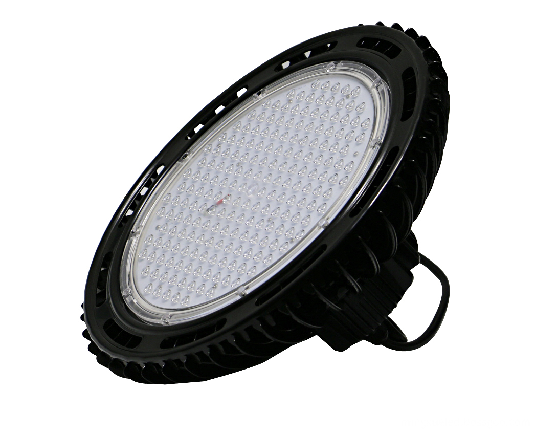
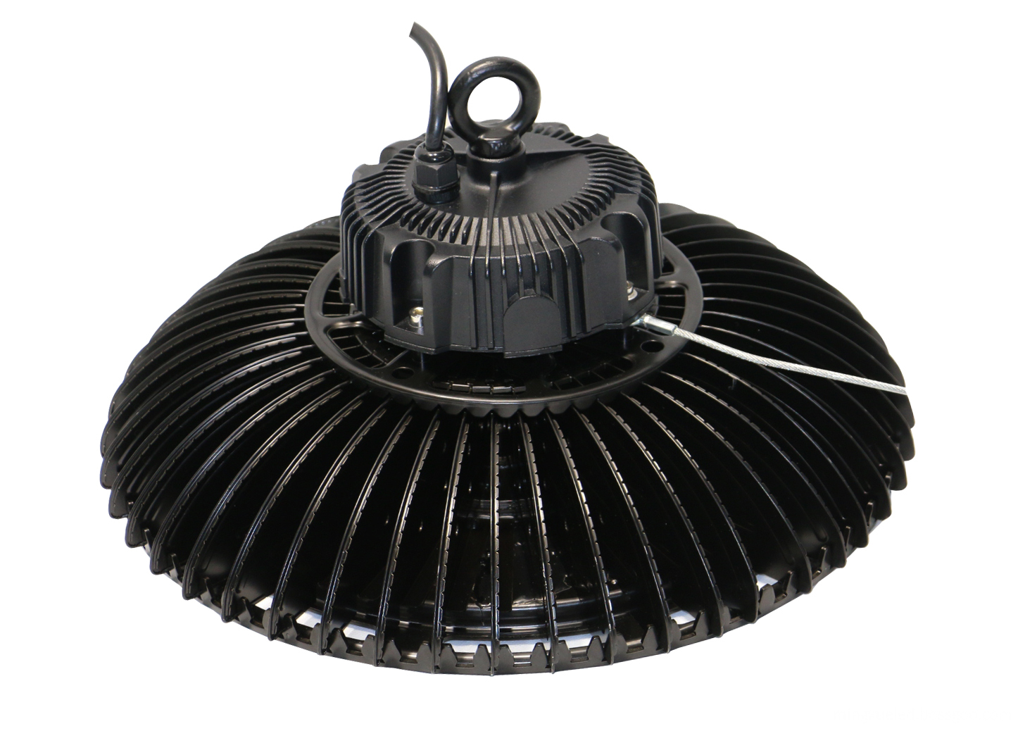
Compared with the traditional mining lamps Led High Bay Light has great advantages:
1 LED high bay high CRI RA> 702 LED high bay high efficiency, more energy, equivalent to 100W of LED mining lamp can replace traditional 250W traditional mining lamp.
3 traditional light fixtures have the disadvantage of high temperature, lighting temperature up to 200-300 degrees. The LED itself is a cold light, lamp temperature is low, more secure.
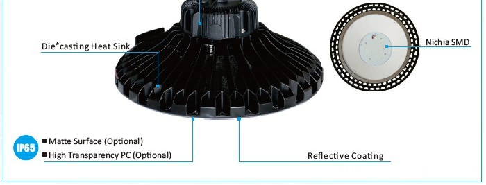
4 LED high bay in constant innovation, the latest model of the finned radiator mining lamp more reasonable heat sink design, greatly reducing the weight of mining lamps, so 80W LED bay light overall weight dropped to less 4KG, and 80-300W LED heat problem perfect solution mining lamp.
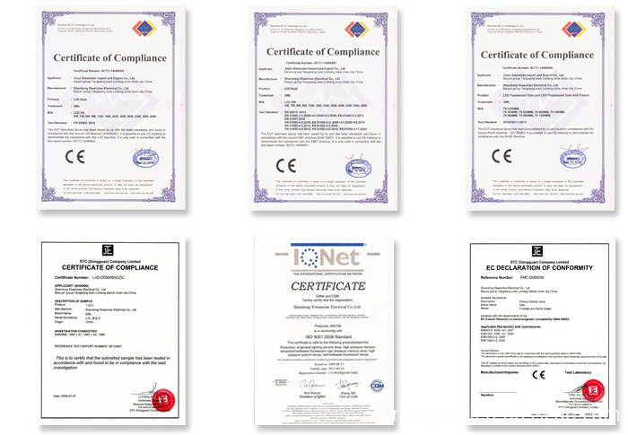
Mingxue Optoelectronics Co.,Ltd. has apply the I S O 9 0 0 1: 2 0 0 8 international quality management system certificate, For LED high bay we apply the CE, RoHS and SAA certificate for our led lighting product.

LED High Bay
Led High Bay,Led High Bay Light,Industrial High Bay Light,Aluminum High Bay Light
Shenzhen Mingxue Optoelectronics CO.,Ltd , http://www.mingxueled.com