In modern integrated circuit chips, the scale of design continues to expand. A system often contains several clocks. One problem with multiple clocks is how to design the interface circuit between asynchronous clocks. Asynchronous FIFO (First In First Out) is an easy and fast solution to this problem. Using asynchronous FIFOs, real-time data can be transferred quickly and easily between two different clock systems. In the network interface, image processing, etc., asynchronous FIFO has been widely used. The asynchronous FIFO is a first-in, first-out circuit used in the data interface section to store and buffer data transfers between two asynchronous clocks. In an asynchronous circuit, since the period and phase between clocks are completely independent, the probability of data loss is not zero. How to design a reliable and high speed asynchronous FIFO circuit becomes a difficult point.
1 asynchronous FIFO working principle and logic block diagram
This article is based on the needs of actual work. A design for constructing a FIFO device using on-chip RAM is given, emphasizing that the design is effective. Reliable handshake signal method for FULL and EMPTY. And implemented on LATTICE's FPGA chip LFXP2-5E. The LFXP2-5E is part of the LATIICE XP2 series and features an optimized FlexiFLASH architecture. Internally contains look-up table based logic, distributed and embedded memory, phase-locked loop (PLL). Engineering prefabricated source synchronous I/O and enhanced SysDSP blocks. There are 166Kbits of EBRSRAM. With its internal EBRSRAM, a certain amount of asynchronous FIFO can be realized without the need to purchase a FIF0 device separately.
As can be seen from Figure 1, the asynchronous FIFO is generally composed of four modules: a data storage unit, a write address generation module, a read address generation module, and a flag generation module. The entire system is divided into two completely independent clock domains—the read clock domain and the write clock domain: the write address generation logic generates the write control signal and the write address in the write clock domain: the read clock domain portion, which is read by the read address generation logic. The control signal and the read address; in the flag bit generation module portion, the read/write addresses are compared with each other to generate an empty/full flag. The operation of the asynchronous FIFO is: on the rising edge of the write clock. When the write enable is active, the data is written to the location corresponding to the write address in the dual-port RAM: on the rising edge of the read clock, when the read enable is active. The data is read in the first in first out order. In case the FIFO is full or empty. Set the full flag FuLL or empty flag EMPTY signal separately. To indicate two special states of the FIFO.
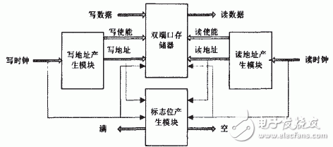
Figure 1 asynchronous FIFO logic block diagram
2 asynchronous FIFO VHDL implementation read clock
2.1 Difficulties in FIFO design
How to synchronize the asynchronous signal so that the trigger does not produce metastability is a difficult point in designing the asynchronous FIFO. A more mature solution to this problem at home and abroad is to use the Gray code for the address of the write address film. This article also uses Gray code directly. Another difficulty in asynchronous FIFO design is how to determine the empty/full state of the FIFO. In order to ensure the correct writing or reading of data. The asynchronous FIFO must be guaranteed to be full. Cannot write: Cannot read in the empty state. The memory is usually organized into a circular linked list.
The principle of the full/empty flag is: the full fill does not overflow. Read more than read. That is, no matter what the situation. There should be no case where the read and write addresses operate on one memory address at the same time. The full flag should be valid when the read and write addresses are equal or differ by one or more addresses. Indicates that the FIFO is full at this time, and the external circuit should stop sending data to the FIFO. Writing data when the full signal is active should be based on the design requirements, or keep, or discard, resend. In the same way, the same is true for the creation of an empty sign. In order to better judge the full/empty flag. A method of adding one bit to the original depth of the FIFO is used, and the Gray code composed of the bit does not represent a new address. That is to say, the 3-bit Gray code can represent the depth of 8 bits. If the highest MSB is added, the Gray code composed of the other three bits does not represent the new address, that is, the 0100 representation of the Gray code. 7, and 1100 still indicates 7, except that the Gray code enters a loop with 1 as the MSB after a cycle of 0 MSB, and then enters a loop with 0 MSB. The other three-digit code is still Gray code. For example: how a FIFO with a depth of 8 bytes works (using a pointer that has been converted to binary), N=3, and the pointer width is N+I=4. Start Rd_ptr_bin and Wr_ptr_bin are both "0000". At this time, 8 bytes of data are written in the FIFO.
Wr_ptr_bin=“1000â€, Rd_ptr_bin=“0000â€. Of course, this is the full condition. Now, assume that 8 read operations have been performed. Let Rd_ptr_bin = "1000", which is an empty condition. The other 8 writes will cause Wr_ptr_bin equal to "0000", but Rd_ptr_bin will still be equal to "1000", so the FIFO is full.
It can be seen from the above. The full flag is generated by the write pointer catching up with the read pointer. That is, after the full write, the write from the zero address is continued until the read pointer is caught. The highest bit of the read/write pointer is different during this period, and the other bits are the same, which is the full condition. The empty flag is generated by resetting or reading the pointer to catch the write pointer. That is, when the write pointer loops to the second round, the read pointer catches up with the write pointer. At this time, the high and low bits of the read/write pointer are the same, which is an empty condition.
Conduction And Convection Dry Herb Vaporizers
END GAME LABS,Conduction And Convection Dry Herb Vaporizers,Portable Dry Herb Vape,Dry Herb Vape Adapter
END GAME LABS , https://www.eglvape.com